

Almost two years after the acquisition by Intel, the deep learning chip architecture from startup Nervana Systems will finally be moving from its codenamed “Lake Crest” status to an actual product.
In that time, Nvidia, which owns the deep learning training market by a long shot, has had time to firm up its commitment to this expanding (if not overhyped in terms of overall industry dollar figures) market with new deep learning-tuned GPUs and appliances on the horizon as well as software tweaks to make training at scale more robust. In other words, even with solid technology at a reasonable price point, for Intel to bring Nervana to the fore of the training market–and push its other products for inference at scale along with that current, it will take a herculean effort–one that Intel seems willing to invest in given its aggressive roadmap for the Nervana-based lineup.
The difference now is that at least we have some insight into how (and by how much) this architecture differs from GPUs–and where it might carve out a performance advantage and more certainly, a power efficiency one.
The Nervana Intel chip will be very similar to the first generation of chips Nervana was set to bring to market pre-acquisition but with the added benefit of more expertise and technology from Intel feeding developments that put the deep learning chip on a yearly cadence schedule, according to Nervana’s first non-founder employee four years ago and now head of AI hardware within Intel, Carey Kloss.
“We did not change much when we joined Intel, but we did utilize a lot of technical resources we didn’t have access to as a startup like packaging, board design resources, power delivery and lab tech, sockets—a lot is still the same but it is beefed up and technologically more advanced,” Kloss tells The Next Platform. Compared to other semiconductor companies he’s worked with, he says the lab bring-up was far faster than anything he had seen and all of leads to more confidence that that yearly cadence for new Nervana Intel integrated products can stay on track with a solid performance curve.
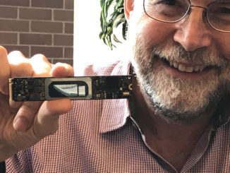
Now that Intel is getting closer to offering “Lake Crest” or what it now calls the Intel Nervana Neural Network Processor (NNP), more details about the hardware architecture are being shared. We have gleaned a few details over the years from Nervana pre-acquisition about what makes their hardware shine against dominant GPUs for training and as of December, now have a much richer sense of how the memory bandwidth bottlenecks are being rerouted to achieve efficient performance.
While there are still no benchmarks since the NNP just arrived back into Intel’s hands, Kloss says that they expect significant performance news in the months to come. Not that it is easy to compare their numbers, of course, with the peak floating point figures for GPUs since the two architectures (while sharing some things in common) operate quite differently in terms of floating point reliance. In other words, it is the forthcoming benchmark suites that will highlight the performance better than trying to map teraflops to teraops for the NNP.
To review and highlight how the architecture stayed essentially the same it’s worth going back to August 2016 when we talked with Nervana just before the Intel acquisition. At that time there were very few details we could glean about the architecture outside of the fact that there were some clever memory tricks at work. As Nervana’s CEO, Naveen Rao told us then following its (relatively) meager $28 million in funding to work to rolled out a 28 nanometer chip by 2017 required some serious legwork. He described briefly the interconnect and memory structure and noted that it would be a contender to the then newly-released NVlink from Nvidia. Rao said then that on a pure operations per second level, the first Nervana chip would go 5X-6X beyond Pascal. “We know people using Pascal now for deep learning, so we have a good sense of the numbers. They’ve introduced NVLink but from the ground up, we engineered a multi-chip solution. Our chip has a much higher speed and a dedicated set of serial links between chips. We also have software constructs to allow the chips to act as one large chip. We threw out the baggage instead of layering onto an existing memory hierarchy, and built something just for this problem.”
All of this remains the same, except the growth of FP16 and more generally, low precision training has become a hotter topic and Nvidia has a new GPU—the forthcoming Volta with the matrix multiplication power of the TensorCore cooked in. Even with these developments, Nervana is on track to have a compelling product when it emerges later this year for wider adoption—but just how much of a performance, efficiency, and usability advantage remains to be seen.
What is new are the long-awaited details about just how the Nervana chip will handle low precision training at scale as well as what that memory and interconnect strategy looks like. Some of these questions were answered with the announcement of Flexpoint, the subject of a detailed presentation at the NIPS conference last month. In addition to the linked paper, there is a slightly more approachable presentation of Flexpoint here. In essence, with the 16-bit integer multipliers and adder trees, the NNP can have both power and area savings compared to the more standard FP16 approach. It is an interesting tradeoff because FP16 has smaller multipliers but with the adder tree and all the shifting required, that wipes out the supposed advantages of FP16, Kloss explains. “We continue to think Flexpoint is the right balance between power efficiency and neural network performance. We have seen that a lot of neural networks are fairly well behaved so that 16 bits of dynamic range is enough and we can get the efficiency benefits of havng fewer shifters and bits of math that require floating point.
“Neural network computations on a single chip are largely constrained by power and memory bandwidth. To achieve higher degrees of throughput for neural network workloads, in addition to the above memory innovations, we have invented a new numeric format called Flexpoint. Flexpoint allows scalar computations to be implemented as fixed-point multiplications and additions while allowing for large dynamic range using a shared exponent. Since each circuit is smaller, this results in a vast increase in parallelism on a die while simultaneously decreasing power per computation.”
The other side of the neural network performance coin for Nervana and Intel is in how the memory and networks lead to improved bandwidth. If you look at the inside of the die as was presented at NIPS, there are both on- and off-chip high speed mesh networks along with high bandwidth memory (HBM). Nervana’s goal was to maximize the area for matrix multiplication and convolutions versus spending that area on other things that are needed to make chips like GPUs fit a wider set of general purpose workloads. With a big enough neural network, this can be expanded using external networks to multiple die with enough bandwidth between those to make all the chips operate as a single giant compute node.
“Matrix multiplication and convolutions are a couple of the important primitives at the heart of deep learning. These computations are different from general purpose workloads since the operations and data movements are largely known in advance. For this reason, the Intel Nervana NNP does not have a standard cache hierarchy and on-chip memory is managed by software directly. Better memory management enables the chip to achieve high levels of utilization of the massive amount of compute on each die. This translates to achieving faster training time for deep learning models.”
Those on- and off-chip interconnects are another key to the architecture’s bandwidth with 1.2 terabits of bidirectional bandwidth through SerDes (serializer/deserializer) links broken into four 100GB “quads”. We do not have an illustration for this, unfortunately. As Kloss tells us, however, this is obviously the key to making several chips act as a single large virtual chip that can expand to meet larger models.
Again, these revelations are not necessarily a surprise since Nervana described what sounded a lot like a fast custom interconnect, high bandwidth memory, and a unique take on precision a couple of years ago. However, it is good to finally see what is inside so we can start making better comparisons between existing approaches to training on the market from giants like Nvidia to the new wave of deep learning chip startups we’ve covered in the last few years.
Intel’s goal for deep learning is to have a product for all implementation sizes. In addition to our conversation about the Nervana Intel chip, he points to recent papers that highlight Xeon CPU only and FPGA training times as well as the Movidius assets for large-scale machine learning inference. Time will tell how much mindshare Intel can pull so long after the initial excitement around Nervana already died down.

Keeping Pace In A Fast-Moving AI Space
During the Intel AI Summit earlier this month where the company demonstrated its initial processors for artificial intelligence training and inference workloads, Naveen Rao, corporate vice president and general manager of the Artificial Intelligence Products Group at Intel, spoke about the rapid pace of evolution in the AI space that …

Former Nervana Leads Target Optimal Training Configurations
Ex-Nervana Systems engineers made the jump from a hardware-centric approach to efficient training to pushing better insight into optimization of models and systems. Nervana Systems was one of the first AI chip startups to generate big buzz, culminating in an acquisition by Intel in summer, 2016. The startup’s co-founder and …

Another Strange Shift for the AI Chip Startup Segment
Few of the AI hardware startups that have made it through the first round of reality (roughly 2016 until the present) have managed to navigate the choppy waters without shifting course, sometimes wildly. Nearly all have a story that begins with training, which washed into a rabid focus on inference …
Be the first to comment