
It has been two years since chip maker Cavium rolled out its ThunderX Arm server processor roadmap and gave us the first glimpse of its second-generation ThunderX2 processors. A lot has changed in that time, and Cavium is now sitting in the cat-bird seat of the Arm server market at just the moment that it is merging with rival chipmaker Marvell.
Timing is everything in this IT racket, and Cavium certainly has been fortunate in this regard.
Thanks largely to Avago Technologies buying Broadcom in May 2015 for a stunning $37 billion and then at the end of 2016 losing interest in Broadcom’s “Vulcan” Arm server processors – perhaps foolishly, perhaps cleverly to avoid antagonizing Intel in the datacenter – Cavium finds itself, after snapping up the assets of those Vulcan designs and the people behind them, with two credible Arm server processors, each able to take a bite out of different parts of Intel’s Xeon processor business.
Cavium is being a bit cagey about the nature of the ThunderX2 product line, but we can confirm that the variant of the ThunderX2 chip that was the hot item at the recent SC17 supercomputing conference in Denver was indeed actually the Vulcan processor, not Cavium’s own ThunderX2 design. Based on the initial benchmark tests and some others we have gotten our hands on since SC17 started, this Vulcan variant of the ThunderX2 has the right balance of compute capacity, memory capacity, and memory bandwidth to take on the “Skylake” Xeon SP Gold series chips announced by Intel back in July in the HPC arena.
It is a wonder why Broadcom did not see the Vulcan chip through and productize it, based on the results that we have seen thus far. But creating a server ecosystem takes time and investment, and Avago, which now uses the Broadcom name, is brilliant at extracting profits out of well-established and mature technologies, such as chips for Ethernet and PCI-Express switching and disk controllers, and is less inclined to take big risks. With its $6 billion acquisition of Cavium, announced last week, Marvell is ready to take those risks and try to build a complete datacenter hardware platform with Arm chips at the center.
Between the time when Broadcom (the original one that is the main supplier of Ethernet ASICs for datacenter switches in the world) announced its intent to build the Vulcan Arm server processors and when it sold off the business to Cavium at the end of 2016, not much was known about the Vulcan chips. Given the intense response to competition regarding datacenter compute expected from Intel, which accounts for the overwhelming majority of processors shipped, all of the Arm dealers were pretty tight lipped. Here is what was promised originally back in October 2013 for the new chip architecture:
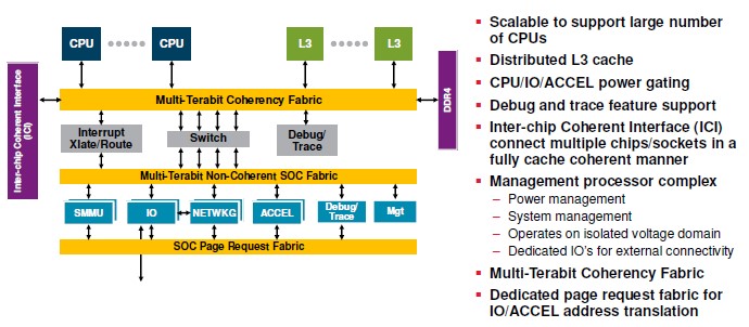
Here is what was promised for the system-on-chip design:
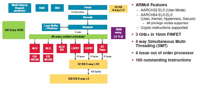
There is a lot in these charts, so let’s walk through it. We suspect that the custom ARMv8 core design and the layout of the SoC stayed mainly the same, but it is possible that Cavium changed the core counts on the Vulcan ThunderX2.
The original idea Broadcom had with the Vulcan chips was to be the first to market with a 16 nanometer FinFET processor. The homegrown ARMv8 core was to have a four-issue, out of order, superscalar core, something akin to a Power7 core, but actually inspired by the NetLogic XLP MIPS-based network processors that Broadcom had acquired several years earlier. Each core was to have four threads – more than the two of a Xeon core but less than the eight of a Power or Sparc core. The Vulcan core had 32 KB of L1 instruction and 32 KB of L1 data cache plus 256 KB of L2 cache. The core could issue for instructions per clock cycle and could have 180 outstanding instructions in flight; it also supported both 32-bit and 64-bit Arm processing modes. (Qualcomm ripped out the 32-bit support in its “Falkor” core on the Amberwing chip to squeeze more cores on the die. Interestingly, the Vulcan core had two Neon floating point units, which together could process four double precision fused multiply adds (FMAs) per clock. The Vulcan cores were intended to run at speeds in excess of 3 GHz.
To make the original Vulcan SoC, Broadcom was planning to gang up the cores and segments of a distributed L3 cache using a coherency fabric that had “multi-terabit” capacity. This coherent fabric also linked out to DDR4 memory controllers on the die as well as to the Inter-Chip Interconnect (ICI), which appears to be Broadcom’s own implementation of NUMA, derived from the NLP network processor family. The Vulcan SoC had a switch hanging off this coherent fabric, which linked on the other side to a multi-terabit non-coherent fabric that in turn had various I/O and networking coprocessors and accelerators as well as system management controllers on that fabric. The Vulcan chip also sported full virtualization of the cores, memory, I/O, and accelerators.
Which brings us to the comparison that Broadcom was passing around under non-disclosure in 2014, pitting the Vulcan chip to the then-current “Ivy Bridge” and “Haswell” Xeon E5 v2 and v3 processors:
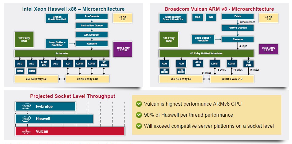
The architecture was similar in many ways to the Xeons of the time, with a much wider table lookaside buffer (TLB) for the L2 cache. The idea was to make the highest performing ARMv8 core and get to 90 percent of the performance level of a Haswell Xeon core and then have more cores than the middle-bin parts that represent the best bang for the buck and the bulk of the shipments in the Xeon line.
A lot of the feeds and speeds of the Vulcan ThunderX2 chip, which is called the CN99XX in the Cavium catalog, as delivered by Cavium are being kept under wraps, but this is what Varun Shah, product line marketing manager at the chip maker, revealed at the SC17 conference:
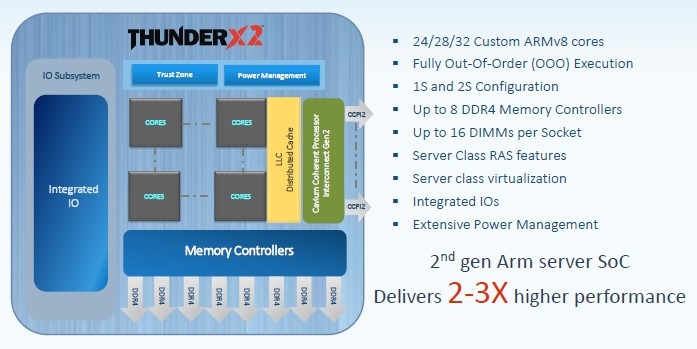
Shah did not divulge the sizes of the L1, L2, and L3 caches on the Vulcan ThunderX2 and said that they would be revealed at some future time. The exact nature of the floating point was also not discussed, but we don’t think any of these have changed since Cavium took over the Vulcan project. What we can see is that the Vulcan die tops out at 32 cores, with variants with 24 cores and 28 cores activated, which is holding toe-to-toe on the core count with the new Skylake Xeon SP processors from Intel. The Vulcan ThunderX2 has eight memory controllers, two more than the six of the Xeon SP, and delivering more bandwidth to the processors. The DDR4 memory controllers on the Vulcan chip have two DIMMs per controller, for a total of 16 memory sticks per socket, and at the moment, the NUMA scalability is limited to two sockets and 32 memory sticks. In theory, that can mean 2 TB of memory per socket, using very expensive 128 GB sticks, but it is far more likely that customers will use 16 GB, 32 GB, and maybe 64 GB memory for 256 GB, 512 GB, or 1 TB of capacity and get the full memory bandwidth just the same. For in-memory computing, there will be a temptation to push up to 1 TB per socket – until the cost comes in. For HPC workloads where simulation and model engines can fit in 64 GB or 128 GB of the main memory, they will be temped to go cheap on the memory and scale out the cluster, as Lawrence Livermore National Laboratory just did with its 125 petaflops “Sierra” system.
It looks like the Vulcan that is being delivered is a bit different from the Vulcan as originally conceived, with the big change being that the NUMA interconnect from the original ThunderX processors has been updated to the Cavium Coherent Processor Interconnect 2 (CCPI2) level and ported over to the Vulcan ThunderX2 chips, allowing for multi-socketed systems. (To be fair, Cavium could be using the Broadcom interconnect that was renamed, or a hybrid of its own CCPI and Broadcom’s ICI.)
The Amberwing Centriq 2400 processors from Qualcomm, which debuted three weeks ago, do not support NUMA shared memory expansion beyond a single socket. And the X-Gene line from Applied Micro, which is now controlled by a company called Project Denver that is in turn owned by the massive private equity company The Carlyle Group, is using a software-based NUMA extension called X-Tend that has yet to be proven in the field as far as we know but which does offer the ability to expand to eight sockets in a single system using X-Gene 2 or X-Gene 3 processors.
Where The Compiler Hits The Code
The precise feeds and speeds of the Vulcan ThunderX2 are still not available, but Shah did provide some guidance on the relative performance of this implementation of the ThunderX2 compared to the prior ThunderX chip as well as against Intel’s Skylake Xeon SP chips.
In general, the Vulcan ThunderX2 has 2.2X times the memory bandwidth, 2.5X the floating point performance, and 3X the integer performance as the original Cavium ThunderX chip, which we profiled back in May 2016 when Cavium and Intel made some benchmark results they had individually run available for Cavium’s first ARMv8 processor. That 48-core part, etched in 28 nanometer processes, ran at 2.5 GHz and probably consumed somewhere around 150 watts to 160 watts; it probably consumed 135 watts at around 2 GHz. This is considerably higher than the 95 watts that Cavium was shooting for with a 2.5 GHz chip. That original ThunderX chip did not have L3 cache, but rather a 16 MB shared L2 cache.
The Cavium ThunderX2 chip, by the way, will debut in 2018 and will sport 54 cores designed by Cavium running at around 3 GHz, with up to 32 MB of shared L2 cache with six DDR4 memory controllers and a coherent fabric linking to various I/O controllers, security, and other kinds of accelerators. It will also, we presume, make use of the CCPI2 NUMA interconnect. (We profiled the original ThunderX2 back in May 2016.) As far as we know, this chip will support PCI-Express 3.0 controllers. That 54 core Cavium-designed ThunderX2 was expected to have 2X the memory bandwidth and integer and floating point performance as the original ThunderX, with 2.5X the coherent interconnect bandwidth and Ethernet networking bandwidth and 3X the speed on encryption and hashing on accelerators. The idea was that this Cavium ThunderX2 chip would have about the same performance of top bin Skylake Xeons on web infrastructure and various cloudy workloads.
Shah did put out some specific benchmarks pitting the Skylake Xeon SP chips against the Vulcan ThunderX2 chips, thankfully, which complement the results we have seen on the prototype of the Isambard supercomputer at the University of Bristol.
As you might expect, given the memory bandwidth advantage it has over the Skylake Xeons, Shah emphasized the performance difference between the Xeon SP and the Vulcan ThunderX2 on the STREAM Triad memory benchmark. In this case, the memory bandwidth was measured on two-socket servers, one using a pair of the top bin 32-core ThunderX2s and another using a pair of the 20-core Xeon SP 6148 Gold processors – a typical chip for HPC customers – from Intel. Take a look:
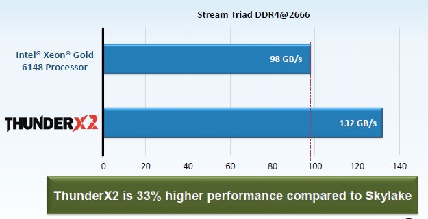
The ThunderX2 chip is delivering 34.7 percent better memory bandwidth as gauged by the test (not 33 percent as the chart says), which is a significant advantage for workloads that are bound in terms of memory bandwidth. (That covers a lot of HPC workloads.)
This chart takes a look at relative performance on SPEC integer and floating point tests, with various compilers used during the tests:
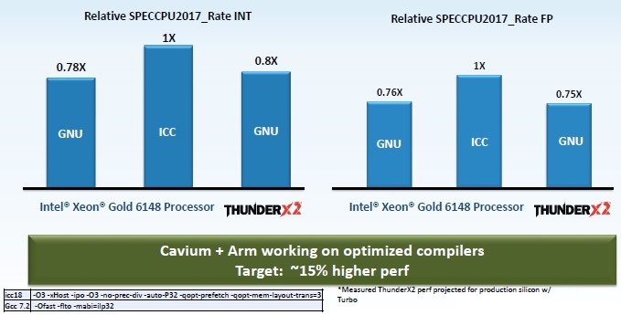
This is very interesting data in that it shows the difference in performance between the GNU open source compilers and Intel’s own compilers on the Skylake processors and then how the Vulcan ThunderX2 stacks up when using the GNU compilers. The fine print there says that Cavium has measured the current performance on pre-production silicon and then projected what it will get from production silicon with the CPU cores running in turbo mode.
As you can see, the 32-core Vulcan ThunderX2 is within spitting distance of the 20-core Skylake when using the GNU compilers, and with Arm and Cavium working on tuning up the Allinea compilers, they expect to be able to goose performance by another 15 percent or so further on these two SPEC CPU 2017 tests. That puts the Cavium chip close enough for government – and other – work on the SPEC tests, which are gatekeepers more than they are something that organizations use to make purchasing decisions.
Cavium has also run a bunch of benchmark tests on popular HPC applications using the GNU compilers, and the Vulcan ThunderX2 stacks up quite nicely against that Xeon SP 6148 Gold processor:
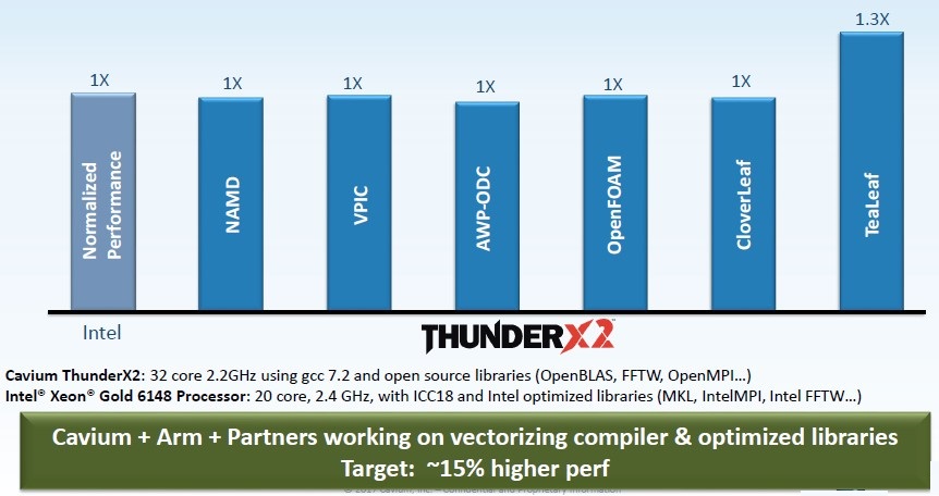
With the tweaks to the compilers, the Vulcan ThunderX 2 should be able to leverage its higher memory bandwidth and larger core counts to get performance even higher. But the competitive Xeon SP chip will probably be in the Platinum band, probably a 24-core Xeon SP 8168 running at 2.7 GHz, which costs a lot more dough.
Shah did not divulge pricing or SKU specifics or power consumption figures for the Vulcan ThunderX2 chips, which we are eager to see. Cavium is sampling pre-production units of the Vulcan ThunderX2 now and will be going into production “in the near future” with the processors, according to Shah.
What seems clear is that Cavium can compete with Intel on performance. And we suspect that is can compete with it on price, too, eating into Intel’s profits as the software ecosystem for Arm processors matures even further. The original ThunderX2 chip will go after cloud and infrastructure where accelerators matter more than memory bandwidth and per-core performance, and the Vulcan ThunderX2 will chase per-core performance and memory bandwidth.
This is going to – finally – get interesting. Live long and prosper, indeed.

Looking Ahead To Marvell’s Future ThunderX Processors
If you are going to take on Intel in server processors, you have to play the same kind of long game that Intel itself played as it jumped from the desktop to the datacenter. And now that Cavium is part of chip giant Marvell and others have exited the field …
Inside Amazon’s Graviton3 Arm Server Processor
The Graviton family of Arm server chips designed by the Annapurna Labs division of Amazon Web Services is arguably the highest volume Arm server chips the datacenter market today, and they have precisely one – and only one – customer. Well, direct customer. These two facts inform the design choices …
The Prospects For An Arm Server Insurrection
If you want to break into datacenter compute in a sustainable way, it takes the patience of a glacier. And not just any glacier, but one that predates the Industrial Revolution. The reason is that IT shops are a conservative lot, and change comes slowly, even when they seem to …
“The homegrown ARMv8 core was to have a four-issue, out of order, superscalar core, something akin to a Power6 core, but actually inspired by the NLP MIPS-based network processors that Broadcom had acquired several years earlier.”
A) It’s XLP, not NLP.
B) Power6 was in-order and dual-threaded. Vulcan looks *nothing* like Power6. It’s closer to a modern Intel core than a P6.
Yup. Meant Power7, not Power6. Yes, Power7 had eight threads per core. Yup, Broadcom (well NetLogic) XLP. I had the name in my head NetLogic Processor.