

We caught wind of the “Aurora” Vector Engine vector processor and the “Tsubasa” system from NEC that makes use of it ahead of the SC17 supercomputer conference, and revealed everything we could find out about the system and speculated a bit about how the underlying processor in the absence of real data. At the conference in Denver, NEC formally unveiled the Tsubasa system and its vector motors, and now we can tell you a bit more about them and how NEC stacks them up against CPUs and GPUs when it comes to floating point work.
Just to be consistent with the many prior generations of NEC vector processors, we are calling the Aurora chip the SX-10+, and indeed it is an eight-core vector processor with a fat chunk of HBM2 memory that links to it using a silicon interposer. The SX-10+ is a kicker to the four-core SX-10, which was delivered in 2015 and employed much slower and less dense DDR3 memory on the system board.
While the Aurora chip is implemented on a PCI-Express card, Shintaro Momose, manager of SX vector supercomputer development within the IT Platform Division at NEC, wanted to make clear that this new hybrid Xeon-SX-10+ system does not use an offload model, but rather uses the PCI-Express bus as an interconnect between Vector Engine cards within a single system and uses 100 Gb/sec EDR InfiniBand as an interconnect across nodes. Conceptually, it is more like the kind of two tier network you see with an interconnect like Cray’s “Aries” which mixes short haul copper cables and long haul optical cables to link nodes together. In a sense, the Xeon processors that are in the cluster are a kind of serial compute offload to the Vector Engines.
Here is what it looks like conceptually as the Tsubaba system scales out:
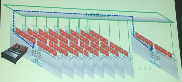
In the example above, the PCI-Express and InfiniBand networks are running a set of firmware in the Tsubasa A300-8 system that is based on a two-socket Xeon node with eight Vector Engines in the eight PCI-Express 3.0 x16 slots in the machine. This firmware allows MPI operations to be directory executed between the Vector Engines in the entire system without copying any of the data or results to the memory in the Xeon portion of the server. The Vector Engines can access the DDR4 main memory in the Xeon compute complex through direct memory access (DMA) methods, but the Vector Engine operating system, as Momose called it, that runs on the vector processors in conjunction with Linux on the Xeon portions of the nodes is designed to minimize the interaction with that Linux kernel as much as possible because of the latencies and overheads associated with depending on the CPU and its memory.
This is an important distinction from the popular – and successful – GPU offload model used with Nvidia’s Tesla accelerators and the CUDA parallel programming environment and the OpenMP and OpenACC extensions that allow for parts of simulation and modeling code that use floating point math to be offloaded from CPUs to accelerators. Because of the way the two-tiered PCI-Express and InfiniBand interconnect in the Tsubasa system is implemented, end users familiar with programming on an SX series vector machine from NEC just use Fortran, C, or C++ just as they normally do and the compilers ignore the “Skylake” Xeon processors in the box unless there is a need to offload serial work to those processors. (There are plenty of applications that will not need to do this.) To be very precise, the NEC stack has full support for Fortran 2003 and partial support for Fortran 2008, for C 11 and C++ 14, and runs the MPI 3.1 protocol for parallelization across nodes. The system uses OpenMP to exploit the parallelism on the Aurora chip – OpenMP 4.5 is supported – and the system has automatic means of vectorizing and parallelizing functions through NEC’s compilers, just like prior generations of SX series parallel vector supercomputers from NEC.
This subtle shift in architecture – making the accelerator form factor become the primary compute – is an important one, and the first time we have seen something like this. We admire its cleverness. And it does not tie NEC in any way to the Xeon architecture. In fact, Momose said that the next iteration of the Tsubasa system would have an Arm processor as its host server serial compute offload rather than an Intel Xeon chip.
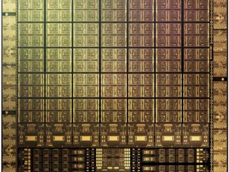
We also admire the engineering that went into this Vector Engine processor. As we anticipated but could not confirm a few weeks ago, the Aurora SX-10+ processor does indeed have eight cores, as shown here:
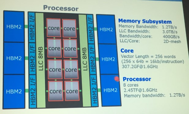
The eight SX-10+ cores are linked to each other with a 2D mesh interconnect that is conceptually similar to that which Intel has created for its “Knights Landing” Xeon Phi and Skylake Xeon SP chips. This 2D mesh also links out to two blocks of L2 cache that weigh in at 8 MB each. Each cache segment has three HBM2 interfaces, which in turn are linked to a block of HBM2 main memory that is stacked eight dies high. With a total of six interfaces, that is 48 chunks of memory at 1 GB a pop, for a total of 48 GB of HBM2 memory for the Vector Engine to play with. This is four times as much memory as Nvidia is putting on its “Volta” Tesla V100 accelerator card. Those L2 caches have 3 TB/sec of bandwidth into and out of the vector cores, and the HBM2 memory has an aggregate bandwidth of 1.2 TB/sec. That works out to 384 GB/sec of cache bandwidth per core and 153.6 GB/sec of memory bandwidth per core – which is a lot. To be sure, the Volta accelerator has a lot more oomph in its complex, but this device has a lot more memory bandwidth coming into and out of it.
That Aurora core has a vector length of 256 words and at 64 bits that is 16 Kb per instruction. A single Vector Engine chip is analogous to having AVX-16,384, to use the Intel nomenclature. The latest Knights Landing Xeon Phi and Skylake Xeon SP processors support AVX-512 (albeit in slightly different ways), which means that the vector units have 512 bits to play with. On the top-bin Skylake Xeon Platinum 8180M part, which has 28 cores, the Xeon socket has an aggregate of 14,336 bits of vector width to play with and running at 2.5 GHz. The Aurora chip has 16,384 running at 1.6 GHz, which yields 307.3 gigaflops per core and 2.45 teraflops per socket.
The SX10+ chip is implemented in a 16 nanometer FinFET process from Taiwan Semiconductor Manufacturing Corp, which also makes Fujitsu’s and Oracle’s Sparc processors and Nvidia GPUs, among many other chips. The Aurora chip is 33 millimeters by 15 millimeters, for a die size of 494 square millimeters, which is 39.4 percent smaller than the 815 square millimeters of the Volta chip from Nvidia. This is one reason why NEC can cram more HBM2 memory onto the interposer than Nvidia can. That interposer, by the way, was designed by NEC, TSMC, and network chip maker Broadcom working together. It consumes under 300 watts at peak load, according to Momose, and we presume that means something between 275 watts and 295 watts.
The Interplay Of Memory And Compute
With any kind of parallel computing environment, there is always an interplay and tradeoff between specialization of the hardware and the software to implement the parallelization. With Xeon CPUs, Momose explained, the hardware is standard and the compilers are standard, but the parallelization is lower and so is the energy efficiency for parallel compute. With GPU accelerators, the hardware and software are both specialized, but the efficiency and throughput are both higher and therefore, in theory and now often in practice, the hassle is worth it.
With the Vector Engines, NEC is saying that customers can use the standard software stack it has offered for years and get the benefits of a GPU offload model without having to do the offload. While the Vector Engine cannot come close to the double precision performance of a Volta GPU, which weighs in at 7.8 teraflops (the number has been tweaked up a smidgen with higher clock speeds since the announcement in May), or offer the many other flavors of compute like Tensor Core dot product engines of 8-bit integer or half precision 16-bit floating point, the Vector Engine does best the Volta when it comes to memory bandwidth, at 1.2 TB/sec compared to 900 GB/sec for Volta, and in memory capacity, at 48 GB of HBM2 compared to 16 GB for Volta.
This ratio of memory to compute, and the need for raw double or single precision floating point, could matter for a lot of workloads. Particularly when the application is specific, like the weather modeling, computational fluid dynamics, data analytics, and seismic analysis and reservoir modeling workloads that NEC is targeting with the Tsubasa system.
To give a sense of the relative benefit of the Vector Engine compared to Xeon and Xeon Phi CPUs and Volta GPUs, NEC revealed the performance of its SX-10+ vector motor on the STREAM memory bandwidth and Linpack matrix math benchmarks:
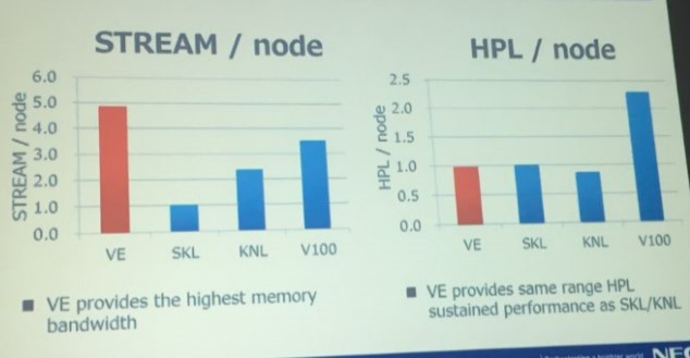
As you can see, the Vector Engine has a lot more memory bandwidth than the processors on a per-node basis (meaning one NEC Vector Engine, one Intel Knights Landing, or one Nvidia Volta per node or two Skylake Xeons per node) and a good bit more than the Volta GPU. The Volta GPUs win hands down on double precision floating point, as we have said. But Momose says that NEC is going to charge a whole lot less for a Vector Engine card than Nvidia charges for a Volta Tesla accelerator, and here is how the price/performance will stack up:
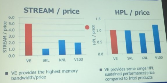
When you throw money into the mix, NEC claims that it is offering 2.5X the bang for the buck compared to Volta on STREAM and almost as much compared to Knights Landing. For Linpack, all of the compute options are in the same price/performance ballpark, with the Knights Landing down a bit (about 15 percent worse) and the Volta better by about 25 percent. So raw floating point is competitive, and memory bandwidth just whips the competition. Again, so long as vector floating point is all you really need.
That is a node performance, but what is important in HPC is how far you can scale out the nodes. The top-end Tsubasa system has 32, 48, or 64 Vector Engines, meaning four, six, or eight of the A300-8 enclosures linked together with 100 Gb/sec InfiniBand. This rack of machines can deliver 157 teraflops at double precision, 76.8 TB/sec of aggregate memory bandwidth, and do so in under 30 kilowatts of power.
Of course, InfiniBand scales a lot further than that. To reach a petaflops of compute would require around six and a half racks and about 191 kilowatts of juice, which is not too bad, and a simple two-tier Quantum HDR InfiniBand switch fabric with a couple of switches could easily handle those nodes (with 40 200 Gb/sec ports or 80 100 Gb/sec ports per switch). To get to exascale, however, is problematic. With the current SX-10+ chip, it would take 6,369 racks of machines and 191 megawatts of juice to hit 1,000 petaflops. A factor of four contraction in the power budget would be better, and a factor of 10X reduction in form factor would still be pushing it.

JAMSTEC Goes Hybrid On Many Vectors With Earth Simulator 4 Supercomputer
Sponsored When it comes to compute engines and network interconnects for supercomputers, there are lots of different choices available, but ultimately the nature of the applications — and how they evolve over time — will drive the technology choices that organizations make. And such is the case with the new …
Argonne Deploying GPU-Dense Testbed Supercomputer
If not for delays, the long-awaited Aurora supercomputer at Argonne National Lab would likely just be coming online. However, with Sapphire Rapids pushed to 2022, the lab is adding to its fleet of large testbed machines, including the forthcoming Polaris system announced this morning. Since Argonne teams can’t test on …
Top500 Supercomputers: Who Gets The Most Out Of Peak Performance?
The most exciting thing about the Top500 rankings of supercomputers that come out each June and November is not who is on the top of the list. That’s fun and interesting, of course, but the real thing about the Top500 is the architectural lessons it gives us when we see …
That the NEC vector engine has a vector length of 256 elements does not imply that there are 256 vector pipelines in the processor. In fact, there are 96 pipelines in each core of this processor. Comparing the vector length of this to a the vector length of a xeon is a misleading comparison. While a long vector length allows many pipelines to work on the same piece of data, a long vector length does not imply performance. NEC vector processors have had 256 element VLs for decades, even back when there were only a couple pipelines.
What’s interesting to me, is that the number of pipelines does not evenly divide into the vector length. 96/256 = 2.67. Thus vector chaining must be required to continuously use all pipelines in the core … or the pipelines are possibly not all meant to operate on the same vectors at the same time. I actually would suspect the latter, as 96 pipelines is a huge jump from the prior generation, and very different from how intel and nvidia arrange their ALUs to attack a problem. I’d love to see the programming guide for this processor.
While the streams performance, and flops per dollar are attractive, I suspect it will be hard to attract customers. The scalar performance of NEC vector processors is notoriously poor, and the software ecosystem for these processors is very small compared to xeon or volta. It’s cool though.
FYI, AVX-512 on the Xeons runs at slower than normal clock speed:
https://blog.cloudflare.com/on-the-dangers-of-intels-frequency-scaling/