

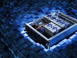
There has been a lot of talk this week about what architectural direction Intel will be taking for its forthcoming exascale efforts. As we learned when the Aurora system (expected to be the first U.S. exascale system) at Argonne National Lab shifted from the planned Knights Hill course, Intel was seeking a replacement architecture—one that we understand will not be part of the Knights family at all but something entirely different.
Just how different that will be is up for debate. Some have posited that the exascale architecture will feature fully integrated hardware acceleration (no offload model needed for codes) with Intel’s own GPU variant. Some see possibilities for an ultra-heterogeneous chip with integrated FPGA (based on the recent Altera acquisition) combined with GPU and other workload-specific acceleration. Others think it might look something like the PEZY processor out of Japan, which is proving its mettle on top-ranked systems with its unique 2048-core design. NEC and others with vector based architectures showcase their wares well on real-world HPC benchmarks. Others still see efforts like Intel’s recent investments in neuromorphic and quantum technologies as indicative of a novel architecture push.
According to Barry Davis, GM of the enterprise and HPC group at Intel, the reality is that this architecture needs to be production ready by 2021, which is not much time, especially if is software footwork required from users. That pares the options down, but also begs several questions about the approach. From what we could gather, a pure CPU is the target—nothing that requires fancy offload models or novel approaches to programming or thinking about problems. The following Q&A we did with Davis seeks to shed light on some of these theories (keeping in mind, NDA briefings on what this will be have only just begun to the wider HPC community at SC this week).
NH: When did your teams at Intel realize there was going to be a change in architectural direction—more specifically, talk about the process of re-envisioning your approach to exascale and what you had to reroute and how?
Davis: I can’t talk about specific dates but I can that as we know, within the last couple of months, the DoE talked about the fact that they are pulling the exascale timeline in to 2021 and that they would be working with us. Subsequently, we said we would take our Knights Hill investments and focus those on this new exascale platform. I can’t say we have been about this for a long time, but we are accelerating.
The architecture we are moving toward for exascale is not something we just dreamed up in the last six months or even year. We’ve been on working on this for a long time. What the two-year pull-in of the timeline to 2021 does is accelerates our roadmap. We could shift quickly to meet that because we’ve been working on this for a while. A two-year pull-in was not easy and we were already trying to accelerate the roadmap before this and consider how to bring in some of the future Xeon implementations and bring those closer into the market. We are not doing something just for exascale; it was something we planned to do, so this is a lot easier to do than it may seem.
NH: Does this boosted timeline to deliver an exascale chip by 2021 change your process roadmap?
Davis: Everything is hitting within a window where we had already targeted that process node in that timeframe. It’s not like we had to say, and this is just an example not a statement about the chip, that to make this work we had to move this from 14nm to 10nm. This was our timeframe for this processor anyway.
NH: Is this software side of this exascale processor story something that will require a lot of lead time for HPC developers to get up to speed with? Are there elements that will be unfamiliar or that will lead to refactoring or changing codes?
Davis: There is definitely an ecosystem here we have to work toward. There is definitely software, but there always is.
It will not be disruptive to the ecosystem but yes, we will have to engage the ecosystem well in advance of 2021 to get codes ready. We are talking to people under NDA about this here at SC17 this week to start that conversation.
Since we are on a CPU path here, this is not going to be a strategy that completely disrupts the ecosystem. We want to run this up the middle with existing models (OpenMP as an example) but there is enablement that needs to happen.
NH: Are there challenges from an Intel production perspective that we haven’t touched on yet—and what, other than software readiness, will be the hurdles for users?
Davis: From an Intel perspective this is a moonshot—this is a big deal. Working without partners to create one of the first exascale platforms in the world is a big challenge. I’m not sure Intel has specific challenges other than we do a lot as a company and the one way to address is to give this importance internally. We address the challenges that are present here daily anywhere in terms of CPU design and packaging and systems—this will exercise all of our muscles. We need to execute this well is the point. We have enough time, this isn’t next year, there’s a few years to figure out what needs to be done and we do that by partnering with the ecosystem and DoE and work together.
From an ecosystem and user perspective, there’s always a software challenge. What will be difficult for people on this one is the question of what makes sense to run at that scale? In other words, what are the applications or workloads that are going to be able to take advantage of this kind of capacity. Which grand challenges? Part of that is integrating everything together. As I said before, modeling and simulation, AI, and high performance data analytics all need to be first class citizens on this platform. You should be able to run all those workloads well and create a workflow that allows the scientist or user to do the task. A good example is running modeling and simulation, then doing AI and then analytics on that and running it all back through—that is all three workloads. It will be hard for users to do that effectively. It changes their thinking about what they do, which used to be one area (modeling and simulation for instance). This isn’t just for exascale, it’s for all of HPC but pronounced on an exascale machine.
NH: What architectural directions seem appropriate for exascale and how did the existing Knights roadmap not fit with that vision?
Davis: We can talk about the right architecture for exascale in general but of course, I can’t be specific [about the Aurora deal] and I’m not going to say “Knights had X and the new Knights has Y”. The needs of the next generation architecture for exascale are fairly well-documented. There’s power, cooling, space, interconnect—and that is a tremendous issue, creating a low latency technology that communicate at that scale. There also compute and storage. There’s a lot to address here.
What we have said publicly is that we are working on a new platform for exascale. That will draw from the best of the Intel portfolio to create a global exascale platform—global because while we’re working with the Department of Energy in the U.S., exascale is a global issue. But what do we need?
We need technology to allow us to compute and accelerate your workloads but do that without specialized code. Everyone talks about accelerators and those are great, but for exascale, every application you bring to that platform should be an offloaded application that you have to port for that particular application. We need something broader that can scale across all of the workloads.
Also keep in mind that the mandate of exascale is to address not just traditional modeling and simulation but also AI and high performance data analytics. You need the right level of performance—and performance per watt across those areas.
NH: There are a lot of architectural contenders right now. How does what you’re working on for the bumped-up exascale chip fit into those?
Davis: You’re talking about hardware architectures but I like to think of things in terms of workloads. So there are, like you say, FPGAs, GPUs, vector machines and things like the PEZY chips in Japan (as one example). Many of those are offload for particular codes that have to be sent over a bus for execution. That’s fine but we are a CPU company. We like to think about codes executing on our platform without the latency and offload. There are areas where that works well, but it doesn’t work for everything and CPUs do.
NH: Based on our conversation so far, it does not sound like we are looking at exotic or novel architectures here—are there novel components? How do your recent investments in truly novel areas like quantum and neuromorphic fit into a current or future exascale (or post-exascale) future?
Davis: The neuromorphic and quantum efforts are from the labs and are great research programs at the bleeding edge of compute. The work we’re doing for exascale is not connected from that perspective. If we are bringing something to the market by 2021 and scale it to this level it can’t be a novel architecture. Those research areas have promise for the future, that’s why we have invested at a future level, but for exascale, we need technologies that are grounded in reality and close to ready for primetime.
There are a lot of processor options; some with volume, some without. There are PEZY machines and there’s volume there and GPUs and there’s definitely volume there. Truly novel architectures mean you have to change how you think about things. As long as tools and applications and development activity is similar to what we know, it is not novel. I can’t say if what we are doing is novel, I’ll let you draw your own conclusions, but to me, novel means big changes for end users and as we discussed, we are not trying to be disruptive to the ecosystem.


A Status Check on Global Exascale Ambitions
As we head toward the annual Supercomputing Conference season we wanted to take a moment for a level-set on exascale. There has been much talk about reaching this pinnacle over the last several years and while plenty of centers say they have reached exascale, that is only for single-precision peak …
Is This The End Of The Line For NEC Vector Supercomputers?
Updated: There is some chatter – some might call it well-informed speculation – going on out there on the Intertubes that Japanese system maker NEC is shutting down its “Aurora” Vector Engine vector processor business. If this turns out to be true, this would mark the end of the vector …
Aurora Rising: A Massive Machine For HPC And AI
As long as great science gets done on the final incarnation of the “Aurora” supercomputer at Argonne National Laboratory, based on Intel’s CPUs and GPUs but not on its now defunct Omni-Path interconnect, people will eventually forget all of – well, most of – the grief that it took to …
It sounds like a recasting of the Xeon Phi architecture that will be better at deep learning than is simply adding mixed precision to their vector units. Davis talks about not offloading or accelerating workloads, so that seems to preclude the use of the Nervana Engine to accelerate deep learning workloads (unless he is playing with semantics on us). Maybe they can wire together modified Xeon Phi cores two ways, a bit like how NVIDIA seems to have created their Tensor Cores. Perhaps one wiring is a more standard Xeon Phi way and the second wiring is a Nervana-like or Tensor-like way, or some other way that is beneficial for deep learning.
Summary: we do not know what to do,.we’ll put more xeons together and do incremental improvements on the bottlenecks.
This move demonstrates that Phy was a failure. Intel has to learn how to collaborate with others vendors that do much better in nonCPU areas such as network, storage and accelerators. All of them are needed for hpc, and intel only pushes his own propietary protocols and punishes the communication standards promoted by everyone else. This limits our innovation.
Well, yeah, if the Phi architecture has been killed then I think it’s safe to say Phi was a failure. Without deep learning it would probably still be around, but I think it would just be losing to GPUs more slowly. This new architecture could be very Phi-like though, unless I’m missing some information that has come out. It could run Phi applications with little change to the code.
But the fact that Intel has been “working on this for a long time” and at the same time has been pursuing FPGAs and Nervana and now have announced the development of a high end GPU, a massive undertaking since they say they are looking to address all the compute opportunities such an architecture would give them, leads me to believe that Intel doesn’t have all that much faith in the long-term strength of whatever architecture they are putting into this exascale supercomputer. Or they just have more money than they know what to do with.
correct, they do not have a clear vision… luckily they have the money… so, they will wait for the next ‘cool’ design from competitors and mimic it… as they always did.
Well Intel just hired Raja Koduri the former head of AMD’s Radeon Technologies Group and Koduri had just finished rolling out that shader/compute heavy Vega 10 base die design that runs the Vega GPU microarchitecture. So Raja’s Vega 10 was a compute/AI first GPU design with the ability to also be used for gaming, at some higher power usage than Nvidia’s gaming only focused GP104 die variants that run the Pascal microarchitecture.
GPUs tend to have a lot less of the OS focused instructions compared to CPUs and are more vector related instructions with some specialized Texture and Raster units in addition to the shader cores that do the FP/INT/ALU workloads and loads of vector math focused ALUs/Shader cores. So Intel hired Raja to create some Intel competition to Nvidia’s GV100 compute/AI designs that run the Volta GPU microarchitecture. AMD’s Vega 20 will have a 1/2 DP FP rate to SP FP rate ratio in 2018 to better compete in the HPC workloads that need DP FP math. So Intel has to be considering some from of GPU accelerator Product and maybe even one with some Tensor Processing Units like Nvidia’s GV100 based GPU designs. Intel could have Raja design a full on vector processor based on a GPU microarchitecture sans any specialized ROP/TMU IP that is mostly used for only graphics workloads.
Intel has begun sourcing a custom Radeon Die from AMD to be included on Intel’s new EMIB/MCM milti-chip packaging IP, but Intel is no different than any of AMD’s other PCIe based discrete GPU AIB partners in that on the Intel EMIB package Intel will only be interfacing its CPU core with the semi-custom Radeon Die via PCIe. So that’s not any Intel Licensing of AMD Radeon/Polaris IP to be directly integrated on Intel’s CPU dies that’s just Intel creating a nano motherboard sort of arrangement that integrates the Intel CPU die(With its Intel in-house integrated graphics) with an AMD semi-custom Discrete Radeon/Polaris die and some HBM2. And that HBM2/GPU die is the only part of the EMIB package using a tiny sliver of silicon interposer(Bridge Chip) embedded in a resin to bridge the discrete semi-custom Radeon GPU die to its single JEDEC standard HBM2 die stack via that Embedded silicon interposer using a 1024 Bit traces wide data path GPU die to HBM2 Die Stack(divided into 8, 128 bit independent channels according to the JEDEC HBM2 standard, with that added 64 bit pseudo channel, half a 128 bit channel), capability under JEDEC’s newer HBM2 standard if so desired and actually made use of).
So Intel appears to be purchasing discrete consumer gaming GPU dies via a semi-custom arrangement from AMD while Intel will have Raja working up some Intel competition to Nvidia’s GV100 based enterprise/HPC compute/AI based products. I do not see Intel even bothering too much with any low margin consumer discrete gaming GPU designs as that’s not really Intel’s MO when considering that it’s Intel’s Enterprise market that produces the majority of Intel’s higher margin revenues. So Raja Koduri’s task at Intel will be to keep Intel from losing too much of the HPC Compute/AI markets share to Nvidia’s GV100 based Volta compute/AI GPU variants where Nvidia’s GV100 and OpenPower’s Power9s could put a whole other level of competition in Intel’s way in addition to AMD Epyc CPUs paired with AMD Vega 10 die based Radeon Pro WX 9100(And WX 9100/SSD variants) and Vega 10 die based Radeon Instinct MI25/variants for the AI/Infrencing markets. Intel has hired in Raja Koduri someone who is similar in the GPU field to what Jim Keller is to the CPU field and that’s a top level GPU specialist with a proven track record.
Intel could decide to at a later time design a discrete GPU for the consumer gaming market but that will be years off in time as Raja Koduri’s first task is to defend Intel from the GV100 Volta onslaught before its too late for Intel to stem the flow of revenue from its cash cow enterprise/HPC/Server, and now AI market business. AI is the new killer application that will drive brand new revenue streams into the professional/enterprise based processors(CPU, GPUs, FPGAs, Other Specialized Processors) market. Google’s TPU(Tensor Processing Units) comes to mind and Nvidia’s GV100 includes TPUs of the Nvidia kind.
We were wondering about the GPU angle too but if you read what Barry is saying–and believe me–he thought carefully about every word of this interview–they are pure believers in the CPU with zero offload, whether its cooked in or not. I feel like this is something that makes sense for consumer devices but to get this in place with the software (there has to be offload built into/hardware offload) by 2019 with an ecosystem for a large breadth of apps that run on X86? Methinks not. I will, of course, eat my words if I’m proven wrong. We are getting more info soon through less formal sources.
Sounds like Intel is changing its exascale architecture in mid-game, while others are probably half-way there to implementing it.
I would be very surprised if Intel succeeds in reaching exascale before IBM/Nvidia, Cray/Cavium, or China.