

Seymour Cray loved vector supercomputers, and made the second part of that term a household word because of it. NEC, the last of the pure vector supercomputer makers, is so excited about its new “Aurora” SX-10+ vector processor and the “Tsubasa” supercomputer that will use it that it forgot to announce the processor to the world when it previewed the system this week.
Here at The Next Platform, we easily forgive such putting of carts before horses – so long as someone eventually explains the horse to us before the cart starts shipping for real. NEC is expected to unveil the Aurora chip and the Tsubasa SX parallel vector supercomputer that uses it at the SC17 conference in Denver next month, so we will fill in the gaps then. In the meantime, we wanted to tell you everything that we have found out about the machine and how it compares to the prior generations of SX systems, in particular the SX-9 and SX-ACE machines that predate it.
Vector engines basically made this category of supercomputer machine until federated NUMA machines, with processors with their own math units and large shared memory spaces across nodes, then massively parallel clusters, and now GPU-assisted fat nodes or extremely parallel X86 machines (lots of cores in the die and lots of single socket dies on the system) took over. Some people forget that for more than two years and for five Top 500 lists spanning 2001 through 2004, the world’s most powerful system, the Earth Simulator created by NEC for as a shared research tool for many Japanese institutions, was a vector machine.
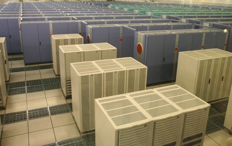
Earth Simulator was based on NEC’s SX-6 architecture, and was comprised of 640 compute elements with a total of eight sockets and 16 GB of main memory per element. The sockets presented themselves as single nodes to the Super-UX Unix operating system that spanned the 5,120 logical nodes in the machine, which had a stunning 10 TB of memory to play with. The system had 700 TB of storage and 1.6 PB of tape archival, and it delivered what was a stunning 35.9 teraflops – yes, that was teraflops – of peak double precision floating point math from those vector engines, and that was enough oomph to run simulations the entire climate of the earth, including the atmosphere and the oceans, at a resolution of 10 kilometers. This was a very big deal at the time, and it is one of the reasons why the Japanese government shelled out $350 million to build Earth Simulator.
In early 2009, the Japanese government upgraded Earth Simulator to the ES2, which was based on the NEC SX-9/E architecture that had made its debut two years earlier – and just as the GPU was gain traction as a massively parallel compute engine to help CPUs do their math homework.
The ES2 supercomputer had a quarter of the compute elements, at 160, than Earth Simulator, and each element had eight sockets as before, each being a single core vector processor. Each of those vector motors had 102.4 gigaflops of peak double precision performance, and the compute element had 128 GB of memory on the board, and all told, the ES2 machine had 1,280 processors and 20 TB of memory with a peak performance of 131 teraflops. Again, this used to sound like a lot of oomph.
The “Project Keisuko” supercomputer was a follow-on to ES2, and it was a collaborative effort between NEC, Fujitsu, and Hitachi with an incredible budget of $1.2 billion. Soon after installing the ES2 machine, the Great Recession was in full roar and NEC and Hitachi were convinced they were not going to make any money on this system, so they pulled out of the project. The original plan was to have Fujitsu donate Sparc64 scalar processors to the cause and mix them with NEC SX vector engines with a sophisticated torus interconnect created by Hitachi to bring them all together into a single system. Hitachi donated the interconnect to Fujitsu, which we now know as the Tofu interconnect at the heart of the K supercomputer at RIKEN, the first machine to break the 10 petaflops barrier. It used Fujitsu’s “Venus” eight core Sparc64-VIIIfx processors, a custom HPC part that is distinct from the enterprise-grade Sparc64 chips Fujitsu had sold at that time.
Because NEC still has customers who want to run applications that have been tuned for vector machines, the company has continued to invest in its SX line. The last big investment came a few years back, when the SX-ACE processor was announced, what would have been called the SX-10 had a rebranding occurred. The chip was unveiled in the summer of 2014 at Hot Chips by Shintaro Momose, manager of SX vector supercomputer development at NEC. This was the first SX chip that had multiple vector units on the same die. To be specific, the SX-ACE chip had four cores linked by a high-speed crossbar with memory access being a core focus of the multicore unit. It looked like this:

And we think that the Aurora SX processor looks very similar, with more cores and a different memory technology. (NEC has not unveiled the block diagram for the chip as yet.) But given that this new chip has a “10” designation in its name, and the SX-ACE would have been called SX-10 if NEC had not changed its naming conventions, we think that the Aurora chip is probably more akin to an SX-10+ kicker and a follow-on to the four-core SX-10 than a whole new design.
In any event, the SX-10 chip as we are calling it had a 1 MB assignable data buffer (ADB) segmented up and parceled out equally to each core. The core actually consists of a vector processing unit (VPU) that can do 64 gigaflops peak that is linked to the ADB by a 256 GB/sec link; off to the side in the core is a scalar processing unit (SPU) that can do four instructions per clock and that is used to do the menial work to keep the VPU fed. Each core on the SX-10 chip has four DDR3 memory controllers assigned to it, with a total of sixteen of them etched on the die and linked by the internal crossbar. That is a large number of memory controllers, four to eight times as much as on a Xeon processor of the time, and it linked out to 64 GB of memory, which is not that much. This is all about bandwidth, not capacity, but 64 GB is not so bad for an accelerator, either.

The SX-10 die has an integrated PCI-Express controller, with two x8 ports, plus an interconnect crossbar (IXS) that has two 8 GB/sec channels to link the SX-10 processors to each other. That ADB buffer has 256 GB/sec of bandwidth, which matches the 256 GB/sec bandwidth across those sixteen DDR3 channels. The vector engines on the SX-10 chip ran at 1 GHz, and delivered 256 gigaflops of peak double precision performance. The SX-10 chip was implemented in 28 nanometer processes (presumably from Taiwan Semiconductor Manufacturing Corp) and had over 2 billion transistors.
The SX-10 card had sixteen DDR3 memory slots, one for each controller, with a bank on each side of the chip like this:
The fun thing is that this SX-10 card above delivered the magical 1 byte per second of bandwidth per 1 floating point operation per second at double precision. (Ahhh, balance.) And it did it all in a 469 watt rate power envelope.
The Big Shift To Big Memory
Here is the big architectural shift that happened between the SX-9 and the SX-10 that is relevant to the new Aurora chip and the Tsubasa system. With the SX-9, a node had a total of sixteen processors on a board in a symmetric multiprocessing (SMP) memory sharing configuration, with a network on the board linking everything together. NEC said back in 2014 when the SX-10 chip was introduced that the memory network in the SX-9 consumed over 70 percent of the 30 kilowatts that the node generated as it delivered its 1.6 teraflops of performance. With the SX-10 design, it took six four-core vector engines to deliver 1.5 teraflops at double precision – almost the same – but it could do so in a 2.8 kilowatt thermal envelope because the memory network was integrated on the SX-10 die itself. That is a 10X reduction in power.
Now, we presume, with the Aurora SX-10+ processor that NEC talked about (but did not fully reveal) this week, the company is scaling up the vector core count while at the same time shifting to a very impressive stack of HBM2 memory akin to that which Nvidia has crammed onto its “Volta” GV100 GPU accelerators.
In fact, Nvidia might be finding itself a little bit envious of the HBM2 memory capacity and bandwidth that NEC has achieved, just like NEC is probably wishing it could have more flops. (There is always a tradeoff in systems.) The Aurora chip has six HBM2 modules on it, with a total capacity of 48 GB, which is four times the 16 GB that Volta has. The SX-10+ has eight cores on it, compared to the many thousands of Volta, and at the top speed of 1.6 GHz, those eight cores on the SX-10+ die deliver 2.45 teraflops at double precision, compared to 7.5 teraflops for Volta. But here is the kicker. The Volta GPU tops out at 900 GB of bandwidth into and out of its four stacks of HBM2 memory, while NEC is getting 1.2 TB/sec of bandwidth out of its six stacks. That extra stacking is yielding 33 percent more memory bandwidth against essentially one third as much compute, for a 10X difference in the balance between compute and memory bandwidth. And the SX10+ module, which is implemented on a PCI-Express 3.0 card of all things, not even PCI-Express 4.0 or something funky like NVLink 2.0 from Nvidia or OpenCAPI 1.0 from IBM, which have 25 Gb/sec signaling that is faster than the 16 Gb/sec signaling used with PCI-Express 4.0 and a heck of a lot faster than PCI-Express 3.0, which has 8 Gb/sec signaling.
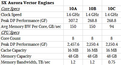
There are three different SX-10+ processor options. The Vector Engine 10A has eight vector cores running at 1.6 GHz and the full complement of 48 GB of HBM2 memory and the full 1.2 TB/sec of memory bandwidth. The Vector Engine 10B cuts the clock speed down to 1.4 GHz on the cores but lets the memory run the same speed, and the Vector Engine 10C cuts the memory in half to 24 GB and the memory bandwidth down to 768 GB/sec. Here are the feeds and speeds of that:
It is funny that NEC is not putting out a variant with only four or six cores activated to increase the usability of its chip yields. It may decide to do that and offer a broader line.
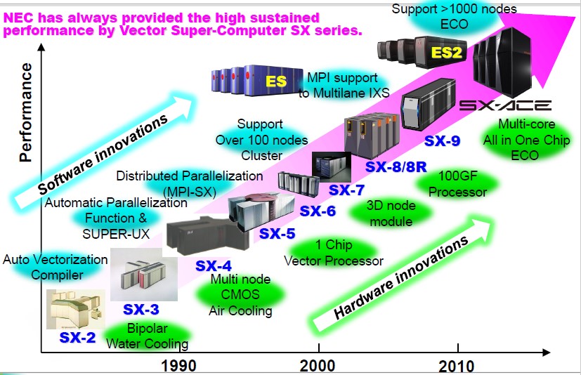
Now, take a look at the evolution of the SX vector processor line:
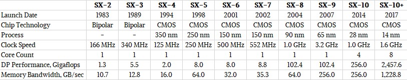
With the SX-10+ vector chip, NEC is increasing the clock speed by 60 percent and increasing the core count by 100 percent, but it is getting nearly 10X the performance out of a single chip. The Aurora SX-10+ chip is rated at 2.46 teraflops, compared to the 256 gigaflops of the SX-10. That is a neat trick, and we want to know how NEC is doing it. The 6X factor of increase in memory bandwidth helps keep that compute fed, but it doesn’t create it.
The Tsubasa Takes Wing
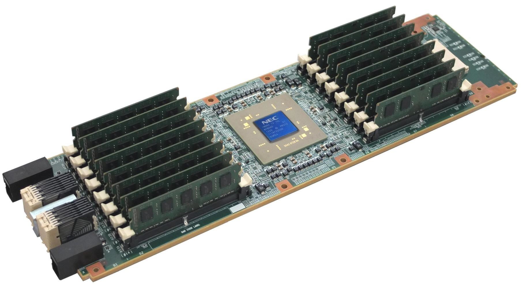
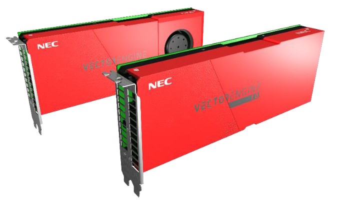
With the SX-ACE Tsubasa system, NEC is taking a hybrid approach that might be like what was possible with the original K supercomputer design. In this case, NEC is taking a two-socket server based on Intel’s current “Skylake” Xeon SP processors and putting one, four, or eight of its Aurora SX-10+ PCI-Express cards, which it calls Vector Engines, into the system. Here is what the Vector Engine cards look like:
NEC has not lifted the covers on this Vector Engine yet, but it is talking about how it is stacking them up inside of systems, much as GPUs are used in hybrid ceepie-geepie machines. (So this is a ceepie-veepie?) The Tsubasa line has a tower server with one Vector Engine, which is not something The Next Platform cares much about except as a development platform that is possibly affordable and therefore can help fuel the vector rebound should it come.
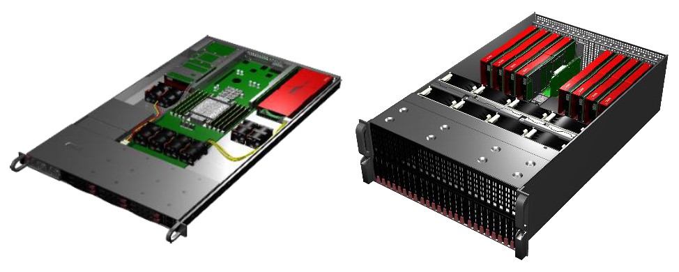
Here is what the two vector Tsubasa A300-2, on the left, and the eight vector A300-8, on the right, look like:
There is also a Tsubasa A300-4 machine with four Vector Engines in a 1U server that will be available, and there will be the big, bad A500-64 system that will take eight of the A300-8 machines and lash them together to create a single vector system image with 64 Vector Engines that will deliver 157.3 teraflops of performance and 76.8 TB/sec of HBM2 memory bandwidth. (Ohhh, the balance is gone. We need to double the HBM2 to 2.4 TB/sec with a dozen stacks.) The fun bit is that this 64 Vector Engine system, which has 512 vector processors, has 3 TB of very fast HBM2 memory to keep it fed and it has a unified memory addressing scheme that spans the Vector Engines and the Xeon SP processors that doesn’t require something like CUDA, according to NEC.
The scalar part of the Tsubasa system is based on Xeon SP Gold 6100 series or Silver 4100 series processors, which are nowhere near the top of the line Platinum 7100 series, which are very pricey and, in this case, are overkill. The nodes are linked to each other using one 100 Gb/sec EDR InfiniBand port, complements of Mellanox Technologies, for every pair of Vector Engines in a system. The top end 64 card Tsubasa A500-64 machine has 800 GB/sec of bi-directional bandwidth across its 32 EDR InfiniBand ports.
What we want to know is how far NEC can scale the InfiniBand to expand the capacity of the Tsubasa system. This could get fun. . . .


Czech Republic Sticks With NEC Vector Engines For Weather Modeling
There are two different Auroras right now in supercomputing. There is the shape-shifting, legendary, and maybe even mythical “Aurora” and now “Aurora A21” exascale supercomputer that was being built by Intel with “Knights” many core processors and now, if Intel can get them out the door, with a combination of …

U.S. Military Looks to NEC to Salvage (Way) Legacy Codes
The era of vector supercomputing might sound like ancient history to some but it’s still deeply rooted in major commercial and government institutions. While it is not optimal or desirable in most cases, the costs and challenges of rewriting or porting old codes that still do heroic work has not …
Couchbase Joins The Vector Search In Database Fray
As we have noted before, vector databases aren’t new even though people talk about them that way, and in fact can trace their origins back a few decades. Exactly when depends on who you ask, but their popularity began to ramp along with machine learning technologies over the past 10 …
As a proud supercomputing dinosaur, I have to take issue with your description of the SX-10 as “balanced”. To really achieve balance, you need 24 bytes/sec per 64-bit FLOP, not 1 (specifically, you need 16 bytes/sec of read bandwidth and 8 bytes/sec of write). Of course, we haven’t seen machines like that in decades.