
In the IT business, just like any other business, you have to try to sell what is on the truck, not what is planned to be coming out of the factories in the coming months and years. AMD has put a very good X86 server processor into the market for the first time in nine years, and it also has a matching GPU that gives its OEM and ODM partners a credible alternative for HPC and AI workload to the combination of Intel Xeons and Nvidia Teslas that dominate hybrid computing these days.
There are some pretty important caveats to this statement, of course. While everyone is excited to see competition returning to the CPU and GPU compute arena, the “Naples” Epyc CPUs and “Vega” Radeon Instinct GPUs are new and it is not precisely clear how they will perform on actual applications. But the basic compute, memory, and I/O of the hardware that AMD is delivering makes it a contended in its own right, particularly with the help of high bandwidth, low latency InfiniBand networking from Mellanox Technologies.
AMD has been winding up its one-two punch in compute for years, and fired off the Epyc X86 server processors concurrent with the International Supercomputing 2017 event in Frankfurt in June, but not actually at ISC17 but in its own event in its Austin development labs. The Vega 10 GPUs, the first in a line of chips that it is pitting against Nvidia’s “Pascal” and “Volta” motors, were previewed in the Radeon Insight Frontier Edition shortly thereafter and formally launched at the SIGGRAPH computer graphics show a week ago along with the commercial Radeon RX graphics cards using the same Vega 10 chips.
While the initial Vega 10 GPUs used in the Radeon Instinct GPU accelerators are going to raise a lot of eyebrows and definitely get some market traction in areas where lower-precision math is preferred, they lack the double precision math that many HPC and some AI workloads require. With subsequent Vega processors, AMD is expected to boost the performance of the Vega GPUs on double precision math, starting with the Vega 20 in 2018 if the rumors are right. Nvidia had similar issues with its “Maxwell” GPUs two generations ago, which had excellent single precision performance but which were never delivered in a version that had high double precision capabilities.
Still, AMD is able to put together a hybrid CPU-GPU compute complex with considerable capacity and technical capability – finally! – and is showing off a bit with ODM supplier Inventec and its AMAX division, which sells gear to end users as opposed to contract manufacturing. The Project 47 demonstration cluster that AMD built in conjunction Inventec/AMAX is a showcase of sorts for AMD’s aspirations in the HPC and AI markets and for its contention that a lot of two-socket Intel Xeon servers fitting with Nvidia GPUs would be better replaced with less expensive and more balanced single-socket Epyc servers with Radeon GPUs.
It has been a long time since a petaflops of compute capacity seemed like a lot for a system, but it is still a lot of number-crunch capacity to put into a single rack. And that is precisely what the Project 47 Epyc-Radeon cluster does. Now, to be sure, when most people talk about HPC workloads, they gauge it in double-precision floating point math, so you have to be careful comparing the Project 47 cluster to any of the machines on the Top 500 rankings of supercomputers, the last of which came out as the Naples Epyc chips were being launched. Still, a petaflops of 32-bit math in a rack is still a lot of compute.
Before we get into the feeds and speeds of the cluster, which will be available in the fourth quarter from AMAX, we need to unveil the specs of the Vega 10 GPU and the Radeon Instinct cards that use it. Some of the characteristics of these cards were unveiled back in July, but now they are out and we can make better comparisons to the Intel CPU and Nvidia GPU components.
The Vega GPU has 4,096 stream processors organized into 64 compute units, and delivers 484 GB/sec of bandwidth into and out of the double-stacked HBM2 memory packed on the interposer for the GPU. (Samsung is the supplier of the HBM2 memory subsystem.) The Vega GPUs used in the top-end Radeon Instinct MI25 card have 16 GB of HBM2 memory on the interposer, and also have dedicated NVM-Express ports that will allow for 2 TB of flash capacity to be directly attached to the GPU accelerator to extend its memory as a kind of fast cache for that GPU memory. That HBM2 memory is four times as much as was crammed onto the prior Radeon Fury X GPU accelerators based on the “Fiji” GPUs and is twice as much as the Radeon RX graphics cards that were announced at SIGGRAPH for gamers and workstation users. Just for fun, and for comparison, here are the specs on these Radeon RX cards, which we think will find use in HPC and AI as well as in gaming because some organizations need flops more than they need memory capacity – or at least they think they do.
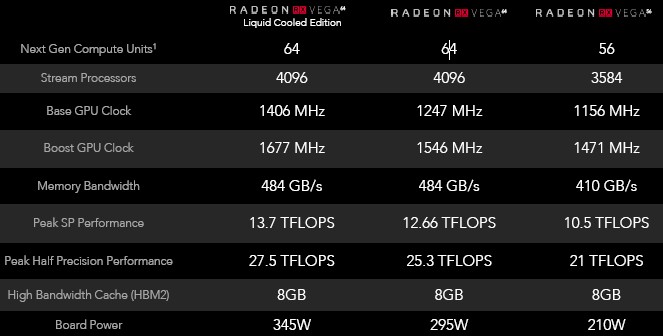
The Radeon Instinct MI25 cards using the Vega GPU have support for half-precision FP16 floating point math, and deliver 24.6 teraflops of FP16 and 12.3 teraflops at FP32; double precision FP64 math units crank through 1/16th level of FP32 oomph with the initial Vega 10 chip, which works out to a mere 768 gigaflops and that is not much performance at all these days. (The future Vega 20 is expected to do a proper 1/2 ratio for FP64 compared to FP32, and that will make it a very zippy device.) The clock speeds for the Radeon Instinct MI25 or Frontier Edition, which runs at a slightly peppier 26.2 teraflops at FP16 and 13.1 teraflops at FP32, were not divulged, but we can guess them based on the Radeon RX table above. We estimate the peak clocks on the MI25 to be 1,502 MHz and on the water-cooled Frontier Edition to be 1,604 MHz. The MI25 and Frontier Edition Radeon Instinct cards both eat two PCI-Express slots in the system and consume 300 watts of juice for air-cooling; the Frontier Edition has a 375 watt water-cooled version that presumably can run more overclocked and deliver more flops. There is not a water-cooled variant of the M125, but there should be.
The HBM2 memory in the MI25 card runs at 945 MHz and has a 2,048-bit interface to deliver that 484 GB/sec of bandwidth. This is lower than the expected 512 GB/sec the card was supposed to deliver, but all vendors using HBM2 memory – including Nvidia – have been surprised that the speed and bandwidth is not as high as it was planned to be. The MI25 has Error-Correcting Code (ECC) on the memory, as does the Frontier Edition, and both have the NVM-Express ports for directly attaching flash memory and maybe someday Micron’s 3D XPoint or some other persistent memory. These features – bigger HBM2 memory, ECC scrubbing, and direct-attached flash – are what make them enterprise products. The Radeon RX cards do not have these features, which is why they are going to be less expensive. And that lower price is why some organizations are going to use them for enterprise workloads even if they don’t have all the bells and whistles.
For the CPU side of the Project 47 cluster, AMD and Inventec chose the top bin Epyc 7601 processor, which has 32 cores running at 2.2 GHz. (You can see the feeds and speed of the Epyc 7000 series chips here.) The Project 47 nodes were configured with only one processor, and instead of needing PCI-Express switches or NVLink interconnect to fan out to the Radeon Instinct GPUs, these just hooked into the system using PCI-Express 3.0 ports. The single-socket Epyc server has 128 PCI-Express lanes, and each Radeon Instinct MI25 card eats two ports of 16 lanes each, so there is no way to link more than four GPUs to the system because that is 128 lanes. The server nodes were configured with 512 GB of DDR4 memory from Samsung, running at 2.67 GHz, and because there were no spare PCI-Express ports, we presume that the flash SSD drives used in the machines – the capacities were not given – were linked to the GPUs, not the CPUs and that the storage for the operating system and system software hung off of SATA ports on the Epyc server motherboards. This is what we would do. Let’s assume that each Project 47 node had 2 TB of flash on each Radeon Instinct card, because this is what is possible according to AMD.
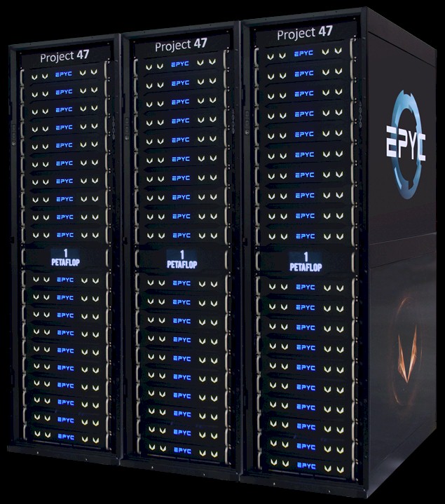
Across those 20 nodes, then, the machine has a total of 640 “Zen” cores humming along at 2.2 GHz. With four Radeon Instinct cards per server, that is 80 cards for a total of 5,120 stream processors with a total of 327,680 Vega cores. Add all of that GPU compute capacity up, and at 12.3 teraflops at single precision, you actually get 984 teraflops peak, not 1 petaflops, but the Zen cores can do some floating point work, too. The Zen core has two floating point units that are 128 bits wide each and that create four pipes that can do two fused adds and two fused multiplies per cycle at 64-bit double precision. So call it eight floating point operations per clock at single precision peak, and at the 2.7 GHz turbo boost speed, that is 21.6 gigaflops per core; across 640 cores in the Project 47 cluster that works out to 13.8 teraflops peak at FP32. So the cluster, in theory, can do 997.8 teraflops. That is pretty damned close to a petaflops, so we will spot Lisa Su, AMD’s CEO during the company’s transformation, that one on the 1 petaflops claim.
That said, the performance on double precision is pretty thin: About 68.4 teraflops. So this is not going to be a very good machine for FP64 work. But it was not designed for that work, and it is very good at what AMD intended it to be good at, which is for remote virtual workstations, render farms, HPC simulations where single precision works (life sciences, seismic analysis, and signal processing are key workloads here), and half precision machine learning training. There is also the possibility of doing 8-bit operations in the new Vega cores, which may prove useful in machine learning and other workloads.
All of the nodes were equipped with 100 Gb/sec ConnectX-5 InfiniBand adapters, and the nodes were linked to one another in a cluster using a 100 Gb/sec Switch-IB InfiniBand switch, both of which come from Mellanox Technologies.
Add it all up and the Project 47 system delivers 30 gigaflops per watt of power efficiency, according to Su, and if you work that backwards, that means the Epyc-Radeon Instinct rack built by Inventec burned about 33.3 kilowatts of juice. That is about as much as you can expect an air-cooled system to cram into a rack and not melt.
For a frame of reference, running double precision Linpack, the most power efficient machine on the planet is the Tsubame 3.0 system at the Tokyo Institute of Technology, which is a cluster of Intel “Broadwell” Xeon E5 processors and Nvidia “Pascal” Tesla P100 coprocessors networked with Intel’s 100 Gb/sec Omni-Path interconnect. This machine encapsulates 3.2 petaflops of peak theoretical performance and burns 142 kilowatts of juice, so its comparable peak efficiency number – the one most like the calculation that Su did – is 22.6 gigaflops per watt. But you have to be careful of these peak numbers since they are, in fact, theoretical. When the Linpack parallel Fortran test was run on Tsubame 3.0, it was able to do just under 2 petaflops at double precision, and its actual power efficiency was 14.1 gigaflops per watt. At single precision, Tsubame 3.0 would in theory be able to deliver 45.2 gigaflops per watt, which is 50 percent better than the Project 47 cluster, but the bill of materials is smaller for the AMD-based system and therefore the cost should also be smaller. Our math suggests that it had better be somewhere around 35 percent cheaper to build a rack of CPU-GPU hybrids to at least to be on par, from a dollars per watt per flops perspective, and it will have to be cheaper still to win deals against Xeon-Tesla hybrids. We happen to think Epyc and Radeon Instinct will be a lot cheaper at street prices, and that server makers using these parts will win deals.
At the SIGGRAPH event, AMD showed off the Project 47 cluster being used as a virtual workstation cloud, and with each Radeon Instinct GPU and each Epyc CPU supporting full hardware virtualization, each node could support 16 users for a total of 1,280 simultaneous sessions. Granted, that was only two CPU cores and four GPU stream processors per user, which is not a lot of oomph. More interesting was Koduri’s demo that showed all of the 20 nodes being coupled together as a giant rendering workstation, and the only jitter on the screen of the rending of a motorcycle was that which came from the network, not from the simulation. All designers will want one of the Project 47 machines as their workstations. . . .
AMD did not show off benchmarks for HPC or AI workloads, but obviously, if the price is right and the flops are precise enough, AMD and its server partners have a chance to win some deals. And next year, it will get even easier as new chippery comes into the field from AMD.
As we have previously pointed out, the “Navi” Vega 20 kicker GPU is expected to be shrunk to a 7 nanometer process and offer double precision at half the single precision rate when it comes to market in 2018. The Vega 20 is anticipated to have the same 4,096 streaming processors and 64 compute units, and the shrink will increase performance by around 20 percent or so, which means single precision will be around 15.7 teraflops and double precision will be around 7.9 teraflops. AMD could shift to four stacks of HBM2 memory for a total capacity of 32 GB, and bandwidth could double or more, depending on a lot of issues with regard to memory speed, power draw, and heat dissipation. The Vega 20 cards are also expected to support PCI-Express 4.0 links, which have twice the bandwidth and will rival the NVLink 2.0 ports that Nvidia has on its “Volta” V100 GPU accelerators in speed.
That also almost certainly means that the future “Rome” Epyc processors, also due next year, will sport PCI-Express 4.0 controllers as well as microarchitecture improvements and a shrink to 7 nanometer processes. So the CPU compute might rise by another 20 percent to 25 percent, perhaps with a mix of IPC improvements, more cores, and higher clocks. And therefore a Project 47 machine using the Rome Epyc and Navi Vega 20 GPUs would deliver around 1.25 petaflops peak at single precision and about 625 teraflops peak at double precision, and be suitable for all HPC and AI workloads to boot.
These kinds of numbers are probably why AMD has been selected as a partner for one of three pre-exascale machines being developed by the Chinese government. That system is being built by Chinese system maker Sugon under the auspices of the Tianjin Haiguang Advanced Technology Investment Co, which is itself an investment consortium that is guided by the Chinese Academy of Sciences.

Making HCI Hay While the Sun Shines
Whenever enterprise server buyers are shopping, they are not just comparing the possible options on the market today against each other. That is important, and we will consider this for a particular workload in the enterprise as we pit AMD EPYC processors against Intel Xeon SP processors. But equally important …

AMD Girds For Compute War With Xilinx Deal
The rumors were right, and AMD president and chief executive officer Lisa Su is indeed printing out a tower of stock to acquire FPGA maker Xilinx for what amounts to about $35 billion and, as it turns out, she is relinquishing her position as president to Victor Peng, chief executive …

HPE And AMD Bag The Big Supercomputer Deal Down Under
Speaking very generally, investment in capability-class supercomputers by national governments tends to scale with gross domestic product. The bigger the particular national economy, the bigger the investment in flops. And so when it comes to Australia, with the highest median wealth per citizen in the world – it jockeys with …
‘These kinds of numbers are probably why AMD has been selected as a partner for one of three pre-exascale machines being developed by the Chinese government.’
AMD was also one of six vendors selected by the United States Department of Energy for Exascale system development under the Pathforward program.
“..Radeon Fury X GPU accelerators based on the “Polaris” GPUs..”
um, what? in what world was furyX running Polaris silicon??
if you’re done the slightest research you’d know it was running Fiji, i mean, its even built on a different (28nm) node rather than Polaris 14nm finFET process.
8GB of VRAM is a laugh there not going to make much inroad on DL with such a low memory config.
The Radeon Pro FE SKUs, as well as the Professional Radeon Pro WX/Instinct SKUs currently offer 16 GB VRAM(2 HBM2 8-Hi stacks), and that’s across only 2 HBM2 stacks. So AMD has already created a design with 4 HBM(first generation) stacks GPU/Interposer with the Fury X (Fiji GPU micro-architecture) based design. So the JEDEC standard for HBM2 allows for up to 8GB per HBM2 stack so 4 stacks of HBM2 would net 32 GB of VRAM on for any Vega based variant should AMD decide it needed that.
There will be Dual Vega/2 dies per PCIe card SKUs offered for the consumer and professional markets and starting with the Vega GPU micro-architecture AMD will be able to use the Infinity Fabric IP to wire those dual Vega GPUs on a single PCIe card designs together for even a faster connection between those 2 dies than is afforded when using the PCIe protocol.
Then there is the fact that even with that 8GB of VRAM under the New Vega GPU micro-architecture that Vega’s new included HBCC/HBC technology can utilize that 8GB of VRAM as a last level cache to leverage the regular system DRAM as secondary VRAM pool with Vega’s HBCC able to perform the swapping in the background to and from that 8GB of HBM2 based VRAM cache to effectively increase the VRAM size to whatever the system DRAM size may be. The Vega GPU IP also includes in that HBCC/HBC/memory controller subsystem the ability to manage in its Vega GPU micro-architecture based GPU SKUs the GPU’s own virtual memory paging swap space of up to 512TB of total GPU virtual memory address space. So that’s 512TB of addressable into any system DRAM and onto the system’s memory swap space of any system NVM/SSD or hard drive storage devices attached. And Vega’s HBCC/HBC manages all that rather effortlessly. There is also the Radeon SSG SKUs that also make use of their own PCIe card included NVM stores for that SKUs needs, and there will be Vega micro-architecture based “SSG” branded variants for both acceleration and AI workloads.
8GB of VRAM is nothing laugh at if that 8GB of GPU VRAM is actually a VRAM cache that can leverage at its disposal up to 512TB virtual memory address space across regular system DRAM or SSD/NVM and only keep in that 8GB of VRAM cache what data/textures the GPU actually requires for it more immediate needs. That new Vega HBCC/HBC IP also has implications for any discrete mobile Vega GPU SKUs that usually come with 4GB or less of total GPU VRAM, so look for an even greater positive gains for any Vega discrete mobile SKUs when they arrive.
I fail to see the any reason to add wider AVX units on Epyc/”Rome” in 2018 when AMD has its Vega GPU IP able to communicate over the Infinity Fabric with its Epyc systems. I can see AMD maybe offering some Zen2 variants with maybe larger/wider AVX units. But with all of AMD’s GPU IP available for FP number crunching, I’d rather see AMD keep its Epyc SKUs saving more power with those smaller AVX units on the CPU cores. And for those that need the extra FP performance maybe AMD developing GPU SKUs with an all double precision shader/cores accelerator product specifically to give AMD’s Current/Future Epyc customers the option of getting their DP FP needs met via an accelerator option.
I’d also like an update from AMD on the development/road-map status of its Workstation Grade Interposer based APU SKUs where the Epyc cores die and the Vega/newer GPU die/s, as well as the HBM2 stacks are all married together on the Interposer with the CPU cores able to via the Infinity Fabric directly dispatch FP workloads to the Interposer based GPU’s NCU(Next-generation Vega Compute Units) using a direct CPU to GPU coherent Infinity Fabric process to feed FP workloads to the GPU and have things managed coherently. There is that Exascale APU research article where AMD/educational institution partner had a very interesting proposal that was funded in part by US government exascale initiative grant money.
AMD’s current Zen(First generation) CPU micro-architecture needs a dancing partner for some heavy DP FP workloads in the HPC markets so AMD has its Vega based SKUs that may only need a variant created that forgoes more 32 bit units on its GPUs for more 64 bit units on some newer Vega variant specialized for DP FP intensive workloads. Vega is not as much a DP FP unit heavy GPU micro-architecture compared to some of AMD’s Pre-Polaris GPU micro-architectures that had higher DP FP resources ratios relative to SP FP resources. the Vega 10 micro-architecture’s Peak Double Precision Compute Performance is around 720-859 GFLOPS dependong on the base clock/boost clock speed of the GPU(Radon Pro FE/liquid cooled SKU). But AMD’s Vega 20 micro-architecture is rumored to up that DP FP ratio from the 1/16th on Vega 10 to maybe 1/2 on Vega 20.
With Polaris and Vega there is less DP FP unit ratios. Maybe AMD can extend that Rapid Packed Math concept in is Vega designs where Vega’s 32 bit FP Units can perform 2/16 bit computations inside each32 bit FP unit’s 32bit ALU. So maybe take it a step further with maybe a single DP ALU able to work on 2 32 bit values. With most server workloads not needing or utilizing Large AVX units as much, I rather that work be given over to accelerator products that excel at DP FP/other precision math and keep the CPU designs more General Purpose in nature.
Amen to the workstation APUs. What a killer product?
Care to fantasize about general configurations, assuming an Epyc size interposer/mcm?
From this next platform article(1) comes this refrennce to an AMD/academic(PDF) research paper(2), and that number 2 refrence will give you an Idea of where Interposer based APUs designs can go, It is a very good read. Silicon Interposers are a bit more interesting than MCMs, as a silicon interposer can not only be etched with thousands of parallel traces, they can also be etched/doped with logic/math circuitry. The whole coherent connection fabric can be made on a silicon interposer and create an active interposer design with which to host the various processor dies HBM2 and whatnot!
(1)
“AMD Researchers Eye APUs For Exascale”
https://www.nextplatform.com/2017/02/28/amd-researchers-eye-apus-exascale/
(2)
“Design and Analysis of an APU for Exascale Computing”
http://www.computermachines.org/joe/publications/pdfs/hpca2017_exascale_apu.pdf
I’ll bet they can’t get that interpose manufactured in serious enough quantities that’s why they are super quiet about it.
It’s interposer not Interpose and if I may interpose for a moment concerning silicon interposers. Those Interposers, of the silicon variety, are just made of the very same material as the processor dies that are(for GPUs)/will be attached to the interposer to create those AMD interposer based APUs. Also note that silicon interposers are in greater numbers being used by more than just AMD/Nvidia and the methods to produce rather large silicon boules necessary for the computing industry’s needs is a rather polished and mature technology. So supplies of the silicon wafers necessary for interposer usage are rather assured by default and can easily be ramped up to meet demand. There is however problems with that reticle limit of current IC lithography IP but as demand for silicon interposers increases so does the economy of scale to allow for some specialized equipment to be designed to get past current reticle limits.
And yes the silicon interposer costs more currently than say an MCM/other IP to produce and have dies mounted properly but there is no better way to get thousands of traces etched onto a single level as opposed to using the fatter traces across the many layered PCBs necessary to compete with any silicon etching processes ability to be etched with thousands of metal traces. One need only look at the BEOL metal traces used on silicon processor dies to realize that any PCB could not have such thin wires made using any of the current PCB process technology.
Now owing to that simple fact that silicon interposers are basically nothing more than dies that are only etched with passive traces currently, we can also extent that to imply that there will be at some time silicon interposers of the active interposer design that will contain actual circuitry. So maybe the silicon interposer will actually comprise a whole coherent connection fabric of 10s of thousands of traces and its associated control circuitry and buffer memory an whatnot. There is really no great technological impediments to making a silicon interposers and creating the equipment to get past any reticle limits other that the economy of scale sorts of things have to come before the increased demand needs are met and that comes via more adoption of the technology for interposer based processor designs used across the larger CPU/GPU/Other processors market place.
It would be a good idea to take the time and read the research PDF listed in the post above your reply and do note that its not at all infeasible to splice 2 interposers together and create a larger area with which to play host to many more processor/HBM2/whatever dies.
Also of note from AMD’s patent filings there is a pending patent for some FPGA in local HBM2 compute with some FPGA die/s added to the HBM2 die stacks for that sort of localized compute that will become important for the exascale markets and on down into the general server/workstation markets and most likely the consumer markets as well. It’s very likely that the Exacale Initiative funding from the US government to AMD/Nvidia/Others will result in some IP that will be utilized across all the relevant processor markets, as always happens when U-Sam/other governments provides R&D matching grants to meet some government needs. I’m relatively sure that Big Blue and its system 360 IP benefited from that sorts of R&D matching government funding when the 360 represented the heights of computing technology back in the day, ditto for Burroughs(stack machines), and Sperry/Others.
I cannot seem to find any details on user settings within HBCC.
We know hbcc allows setting a portion of system ram AND a segment of nvme storage space on a raid array, but i dont know if multiple storage devices can be allocated to hbcc use. An array AND a single nvme ssd e.g.
we also know that for big sequential read/write operations, raid 0 in arrays of up to 7 drives can provide massive, ~memory like bandwidth, on TR/Epyc.
We also know, that for random i/o of smaller files, raid is little better? than cheap and plentiful single nvme nvme ssdS.
Putting aside subjective and wrong opinion on latency being a universal deal breaker for nvme, then if, IF, extra latency does not preclude nvme from being useful as a cache “memory” extender in all apps, then….
My question is, does hbcc allow users to specify only one storage device as a cache extender, or can hbcc ~intelligently manage multiple storage resources in its pool of cache resources?
If so, it would improve hbcc if the powerful array could focus on large sequential r/w, and use supplementary secondary device(s) when an array has no great advantage.
Just as hbcc decides between using fast but limited system ram and vast but slower nvme storage to extend gpu cache/memory address space, may it also decide between multiple storage resources with different properties?
PS, further, what of multi gpuS? Can each gpu be configured separately? Could each gpu have a discrete nvme allocated to its cache pool e.g if it suits?
any links I could check?