

The “Skylake” Xeon SP processors from Intel have been in the market for nearly a month now, and we thought it would be a good time to drill down into the architecture of the new processor. We also want to see what the new Xeon SP has to offer for HPC, AI, and enterprise customers as well as compare the new X86 server motor to prior generations of Xeons and alternative processors in the market that are vying for a piece of the datacenter action.
That’s a lot, and we relish it. So let’s get started with a deep dive into the Skylake architecture.
We dug into many of the higher-level details of the Skylake chips way back in May 2015, when we got our hands on an internal Intel presentation revealing the plan for Skylake and the related “Purley” server platform, and we covered the somewhat complex product segmentation of the chips when it was unveiled this May. With our coverage at the July 11 launch, we focused on the product segmentation – Platinum, Gold, Silver, and Bronze – and revealed the basic feeds and speeds of the 51 variants of the chip and how there were three basic variants of the Skylake that now covered what was formerly the Xeon E5 and Xeon E7 product lines. Intel may have converged the Xeon E5 and E7 chips into a single socket, but there are still 51 versions of the Skylake Xeon SP chip that are publicly available and probably another dozen or so custom versions that hyperscale and OEM customers have asked for. All of these chips differ from each other on a large number of vectors, including number of cores, clock speed, L3 cache capacity, number and speed of UltraPath links between sockets, number of sockets supported, main memory capacity, and the width of the AVX vector units, just to name the biggies.
Before we get into all the details, let’s talk about the Purley Xeon platform – meaning the complete server package as created by Intel – for just a minute.
It’s All About The Platform
The architecture of Skylake is very different from that of the prior “Haswell” and “Broadwell” Xeon chips, and will be carried forward with the next-generation “Cascade Lake” processors that will very likely be implemented in a highly tuned 14 nanometer process – what Intel calls 14++ nanometer in its chip manufacturing presentations. (We had not heard of Cascade Lake before, and assumed future Xeons would be based on the “Kaby Lake” design already implemented in the Xeon E3 chips for single-socket servers.) The point is, the Socket P form factor for Xeon SP processors will be used for at least two generations of server chips, and possibly more. We think Intel will be under intense pressure to increase the I/O bandwidth into and out of the socket, particularly with AMD’s Epyc processors offering 128 lanes of PCI-Express 3.0 on both single-socket and two-socket machines, and that this will require a new socket and very likely a new platform beyond Purley.
Intel has not said much about Cascade Lake, but what we do know is that the “Apache Pass” Optane 3D XPoint memory sticks in the DIMM form factor are now expected to come out in 2018 along with the Cascade Lake Xeon update, and that probably means later in 2018 rather than earlier given the fact that the Skylakes are just shipping. Intel had, of course, expected for the Optane DIMMs, which plug into regular memory sockets and behave like DDR4 memory except they are slower and offer persistence of bits when the power goes out, to ship with the Skylake chips and the initial release of Purley. Intel was focusing on memory expansion, not I/O expansion, and AMD has successfully exploited this by offering 2 TB of memory per socket (most Skylakes top out at 768 GB and only selected models can support 1.5 TB) and up to 128 lanes of PCI-Express traffic for machines with either one or two sockets (compared to 48 lanes per socket with the Skylake Xeons).
How much AMD will be able to leverage this difference in memory capacity and I/O and memory bandwidth remains to be seen. We have not heard of any hyperscalers buying Epyc chips in high volume, but that doesn’t mean it didn’t happen. It sure did happen, however quietly, with the hyperscalers the first time around with the Opterons a decade ago. It could be happening again right now, and we would be none the wiser until we see a bump in AMD server chip revenues. We also think that AMD would be wise to source some 3D XPoint DIMMs from Micron Technology, Intel’s development and manufacturing partner for flash and 3D XPoint memory, so it does not give Intel an advantage next year in overall DDR4 plus 3D XPoint memory capacity.
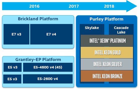
The Purley Platform has incremental improvements on many fronts compared to the prior “Grantley” Xeon E5 and “Brickland” Xeon E7 platforms. The UltraPath Interconnect (UPI) ports that link multiple sockets together to create NUMA configurations with two, four, or eight processors in a single system image run a bit faster than the QuickPath Interconnect (QPI) ports used on prior generations of Xeons since the “Nehalem” launch in 2009. The QPI links used in the “Broadwell” generation of Xeons topped out at 9.6 GT/sec and the UPI links, which have an improved messaging protocol that crams more data into each packet, runs at 10.4 GT/sec at full speed. The new protocol offers anywhere from 4 percent to 21 percent better data efficiency per wire, Akhilesh Kumar, CPU architect for the Skylake chip, tells The Next Platform, and coupled with the 8.3 percent throughput of the UPI links, the NUMA coupling is that much together and therefore machines with multiple processors will run a smidgen more efficiently and look that much more like a giant virtual CPU than those using QPI links.
We think Intel will pull aside one or maybe even two of these UPI links to attach accelerators, such as Altera FPGAs and Nervana machine learning chips, to the Skylake and Cascade Lake Xeons in hybrid systems, giving it an alternative to the NVLink interconnect developed by Nvidia in conjunction with IBM. It would be interesting to see the FPGAs and Nervana chips implemented with their own UPI links so they could be coupled together, but we have not heard of such a thing being on a roadmap.
The Purley platform is comprised of two, four, or eight Socket P sockets, which are linked to each other gluelessly using the integrated NUMA circuits on the uncore portions of the Skylake chips. Specific models of the Skylake Xeons have two, four, or eight sockets enabled, which we detailed in our original Skylake coverage a few weeks ago. The block diagram below shows the configuration of a Purley machine with two sockets:
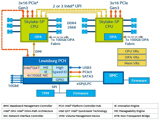
All of the Skylake machines use a “Lewisburg” C620 chipset as the I/O southbridge to hook out to four 10 Gb/sec Ethernet ports, which by the way support the iWARP InfiniBand-over-Ethernet encapsulation method of providing Remote Direct Memory Access (RDMA) across the fabric rather than the RDMA over Converged Ethernet (RoCE) method preferred by many Ethernet switch and network adapter chip makers. The Lewisburg chipset integrates the same chippery that comes from Intel’s X722 external adapters, says Jennifer Huffstetler, director of the datacenter product marketing group at the company, says that this was the best way to lower CPU utilization and boost effective bandwidth for the Skylake chip’s integrated networking. She added that Intel expects that over 65 percent of the server ports that ship in 2017 and 2018 will be running at 10 Gb/sec, so this meets the market need. Those who need 25 Gb/sec, 50 Gb/sec, or 100 Gb/sec ports coming off their servers will have to go to external adapters.
Some of the Skylake Xeons have integrated Omni-Path ports on them, and these hang directly off of the CPU and make use of dedicated PCI-Express lanes that are not exposed for other I/O use. So our guess is that this takes eight lanes of traffic to support at 100 Gb/sec using PCI-Express 3.0, and that means the Skylake chip with 64 total PCI-Express lanes overall, not the 48 lanes per socket in the spec sheets, has some extra bandwidth hidden in it that might be exposed later in the Cascade Lake Xeons.
There was an outside chance that Intel might get at the front of the line and support PCI-Express 4.0, which runs at twice the speed and provides twice the bandwidth as PCI-Express 3.0, but Kumar says that the spec, which was just finalized, was not ready for primetime. IBM’s desire to support PCI-Express 4.0 on the Power9 chips may be one of the reasons why the chip did not launch around the same time as the Skylake and Epyc chips, as was widely expected.
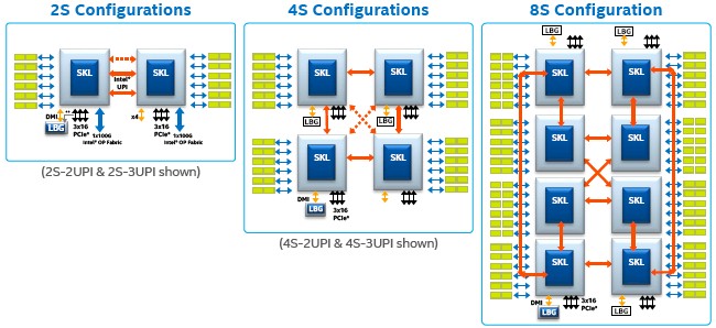
The Xeon E5 chips had two QPI links, which meant it could support machines with two or four sockets, depending on the topology chosen, and the Xeon E7 chips had three QPI links, which meant it could support machines with two, four, or eight processors, again dependent on the topology. Some of the Skylake chips have two UPI ports activated and others have three UPI ports, so the same rules apply, as shown:
Customers who need more NUMA scalability than is inherent in the on-chip NUMA will have to rely on external node controllers developed by third parties for this capability, and it is not at all clear that anyone other than Hewlett Packard Enterprise, with kickers to its acquired SGI UV300 and UV3000 systems, will do this. There has been no indication that HPE will support Superdome X machines running Skylake or Cascade Lake chips, and Dell has shown no interest in creating its own NUMA chipsets to extend beyond the basic NUMA in the Xeon family. Neither has Lenovo, Cisco Systems, Fujitsu, NEC, Bull, Oracle, or Inspur, and that about covers all the big bases in the enterprise.
Digging Into The Microarchitecture Tweaks
The Skylake chips is what we used to call a “tock” in the old “tick-tock” parlance that Intel used to use until it went to a three step “tick-tock-clock” method we have discussed recently. The tick was a manufacturing process shrink, the tock was an architectural change, and the idea was to not try to do both at the same time. Now, Intel is using three stages of process refinements and adding in an architectural bump in the middle and perhaps at the end as it sees fit. (Hence, or naming it tick-tock-clock.)
The point is, a lot of things inside the Xeon core and in the uncore areas that wrap around the cores, changed with the Skylakes, and this was exactly what we expected.
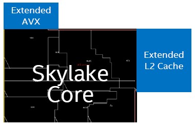
The core at the heart of the Skylake Xeons is not precisely the same as the one used on the Core desktop chips, although Kumar did confirm that the new Core i9 “Skylake-X” high-end processor for gaming machines and technical workstations does use the server variant of the chip rather than the desktop variant.
With all of the tweaks in the Skylake core, the normalized instructions per clock (IPC) has boosted by about 10 percent – we were expecting about 8 percent, so Intel, you win – and that is consistent with past chips that were focused largely on microarchitecture improvements, which includes the Nehalem, Sandy Bridge, Haswell, and Skylake chips in recent generations. The Penryn cores didn’t do much in terms of microarchitecture, and the Westmeres did nothing but add cores; Ivy Bridge and Broadwell had some modest IPC tweaks of around 5 percent.
The AVX-512 vector math units that come with the Skylake Xeons are not just a block copy of the AVX-512 units that were created for the “Knights Landing” Xeon Phi chips that launched last year and that were the first Intel chips (server or otherwise) to support such wide vectors. Despite the very different implementation, the two ways of delivering AVX-512 are instruction-level compatible and therefore applications do not have to be tweaked to run on either Knights Landing or Skylake. It just works.
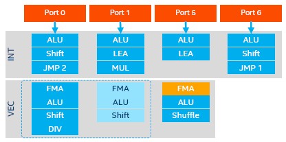
The trick that Kumar and his team came up with to add AVX-512 to the Skylakes is clever. Rather than block copy the AVX math units in Knights Landing, Intel rather fused the two 256-bit math units on Port 0 and Port 1 of the core to make a single 512-bit unit and then bolted a second fused multiply add (FMA) unit onto the outside of the core on Port 5 that delivers the second unit. So the net result is that the chip can, with both FMAs activated, process 64 single precision or 32 double precision floating operations per clock. Here is what the block diagram for that looks like:
We will be going into the performance of these AVX-512 units on Skylake in a separate story focusing on the HPC aspects of the chip.
As you can see, there is not just this extra AVX-512 unit hanging off the base Skylake core, but also an additional chunk of L2 cache. For as long as we can remember, Intel has had 256 KB of L2 cache per core, but with the Skylake Xeons, this is being quadrupled to 1 MB, and it is being done by hanging 768 KB of extended L2 cache on the outside of the core. The L1 data and instruction caches on Skylake are the same at 32 KB each, but the L1 data cache has its load and store bandwidth doubled so it can do two 64 byte loads and one 64 byte store per cycle.
The L2 and L3 caches on the Skylake are organized differently, and these tweaks are only available in the server variants of the Skylake chips just like the integrated mesh architecture is also only used on the server versions. (More on that mesh in a moment.)
With prior Xeon processors, each core had its own private L2 cache that weighed in at 256 KB, and each core also had a 2.5 MB segment of L3 cache that was roughly associated with that core. With the prior Xeons, the shared L3 cache was inclusive, which meant that the L3 cache had copies of all cache lines in the L2 caches. But with the Skylake Xeons, Intel has shifted to a non-inclusive L3 cache structure, which means that the L2 cache lines may not be in the share L3 cache. The other big change is from a shared, distributed L3 cache that was created from those segments to a private, local L2 cache that is tightly coupled to each core and that uses the shared L3 cache more like an overflow cache. The L3 cache for the Skylake Xeons is considerably smaller, at 1.375 MB per core, but the L2 cache is bigger and compensates for this. The overall effect, says Kumar, is that the caches can better feed the cores, and this is particularly important for virtualized and multithreaded workloads, which were spending a lot of time going out to L3 cache and hitting the uncore regions of the chip. The downside is that the L2 cache latency has increased by two cycles, but the larger L2 cache more than masks this latency.
“The larger L2 cache is helping a lot and the smaller L3 cache is not hurting that much,” as Kumar puts it.
Here is a rundown on the microarchitecture tweaks that lead to that 10 percent IPC improvement on the Skylake Xeon core compared to the Broadwell core:
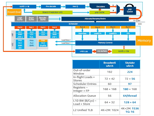
Intel has a larger, and improved, branch predictor at the heart of the core, plus a decoder with a higher throughput and a larger out-of-order window for that branch predictor that allows it to extract more instruction-level parallelism out of applications. The divide and square root functions have higher throughput and lower latency, and the instruction scheduler and execution units also run better. The prefetcher is more efficient, and as we said above, the load/store units have deeper buffers and more bandwidth.
The really big architectural change is not in the cores, but in the way that they are lashed together to share cache memory, UPI ports, PCI-Express controllers, and access to the southbridge chipset that fans out to other I/O devices. This new mesh interconnect borrows some ideas from the mesh that was first deployed on the Knights Landing Xeon Phi, but it is different, according to Kumar.
Only last year we were assured that the ring architecture used for the Sandy Bridge through Broadwell Xeons had some more years of life in it, and the architect for the prior Xeons, Chris Gianos, hinted there would be higher orders of connectivity and maybe something like the mesh in Knights Landing. The Broadwell chips had two nested loops of rings linking everything together, like this:
Kumar tells us that supporting six columns of core on the Skylake die would have required three sets of rings, and that this would be a very big challenge to lay out and would add to latencies and also be a bottleneck for access to main memory and cache memory. Hence the mesh architecture, which is something that many massively multicore processors have employed in the past for this very reason. Here is what the mesh looks like on the XCC, or extreme core count, version of Skylake looks like:
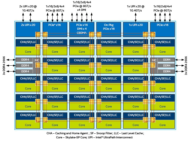
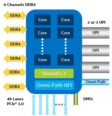
The DDR4 memory controllers hang off the sides and each socket has three ports that support two memory sticks each at a maximum speed of 2.67 GHz. Intel is no longer supporting three memory sticks per socket, and has dropped the memory buffering scheme that was used on the Xeon E7 line to boost capacity and compensate for latency issues in accessing that larger and usually slower main memory.
Across the top of the chip are the three UPI ports – there is clearly room to do four, which would allow for accelerators to be linked in or for NUMA scalability to be pushed higher. There are four PCI peripheral controllers, each with 16 lanes of traffic running at 8 Gb/sec each. One of these controllers is used solely for the integrated Omni-Path network interface on those models of Skylake that sport them, so that leaves 48 lanes that can be used for other things. One of the PCI-Express controllers also has the four-lane Direct Memory Interface (DMI) link that hooks the chip to the Lewisburg C620 southbridge chipset. The Skylake mesh is organized as rows and columns of interconnect, which makes it a 2D mesh architecture by definition, and in the case of the Skylake XCC die, it is a 6×6 mesh.
“What this architecture does is remove any of the bottlenecks and choke points that we would have had otherwise, and it gives us a much more scalable and modular way to keep extending the architecture going forward,” Kumar explains. “This mesh puts us on a different foundation, and it is a significant change to the architecture and the overall organization of the chip.”
This begs the question as to why Intel chose to do rings, and then interconnected rings, in the first place. With the Nehalem through Sandy Bridge chips, a ring worked just fine and a mesh was not needed, but somewhere around Ivy Bridge Intel did in fact debate going to a mesh, and we think the company decided to test it out on Knights Landing first to work out the architectural issues, and that is what HPC is precisely for. To test out ideas before they get to the wider adoption in the enterprise.
This 2D mesh in Skylake operates at the same speed as the L3 cache, and it ranges from 1.8 GHz to 2.4 GHz, depending on what the chip is doing and how thermally stressed it is. There are mesh agents on each core and cache segment in the Skylake chip as well as on every other element on the die. It is hard to make precise comparisons between the rings and the mesh because Broadwell was not implemented with the mesh and Skylake did not use rings, but Kumar says that the mesh has much lower latency and much higher bandwidth between the elements of the die, and it would have to if there are more cores and faster memory and more and faster caches. The mesh also needs this extra oomph so more cores, cache, memory, and I/O capacity, very likely running at higher speeds, can be incorporated into future Xeon chips. Equally importantly, the lower latency and higher bandwidth compared to the rings means the interconnect on Skylake is using less power than it might otherwise, although it will probably be cranked up in future Xeons. The upshot for Skylake is that more of the power can be shifted to the cores, which can run faster and for a longer time.
That leaves memory, and this would be a much more interesting thing if the Optane 3D XPoint DIMMs were available with the Skylake Xeons. But they are not. That said, the Skylake Xeons sport about 64 percent more memory bandwidth compared to the Broadwell Xeons. Take a look:

This particular test was using the STREAM Triad suite of memory bandwidth tests. The I/O bandwidth has increased around 50 percent for the Skylakes over the Broadwells, and this is in line with the increased memory bandwidth. The core count only went up by 17 percent, though, from 24 cores with Broadwell and 28 cores with Skylake, and we suspect that the overlapping ring interconnects were actually a bottleneck. We would not be surprised to see the Skylakes do quite well on some benchmark tests compared to their predecessors because of this. We will be getting into Skylake system performance on all kinds of workloads shortly, so sit tight.

Debunking Datacenter Compute Myths, Part Two
Welcome to the second part of our Debunking Datacenter Compute Myths series. In the first part of this series, which you can see here, as well as in this second part, The Next Platform sat down with Lynn Comp, vice president in AMD’s server business unit, to talk about some …
Intel Sometimes Charges A Hefty Premium For Sapphire Rapids
No matter what, and without any excuses about Moore’s Law slowing down, those buying compute, storage, and networking expect at least one thing in any generational leap in a device: That the cost per unit of capacity goes down. And for the hyperscalers who run massive applications, they look at …

Mixed Results For The Datacenter Thundering Thirteen In Q4
We have been tracking the financial results for the big players in the datacenter that are public companies for three and a half decades, but starting last year we started dicing and slicing the numbers for the largest IT suppliers for stuff that goes into datacenters so we can give …
“This begs the question as to why Intel chose to do rings, and then interconnected rings, in the first place.”
afaik, because more cores means unsustainably more data hops.
In the great race between Intel and AMD, Supermicro has EPYC 2P board available through open market channel waiting their open market processors.
Intel SP showed up second week after the formal introduction. In the first four weeks, open market supply across all SP grades is 3.5% of Broadwell 26xx v4 during fourth week and 4.6% of Haswell 26xx v3 in fourth week of supply;
Skylake SP are 68.8% silver/bronze, 30% gold, 1.1% platinum. The most prolific grade is Silver 4112 into storage server with HP already available from open market, not sure what that says exactly, followed by Silver 4008.
Most prolific gold grade is 6130 at 7.7% of all grades followed by 6134 and 6128.
All Xeon Skylake SP in week are 0.3067% of available Broadwell v4 in week that is 32,498% more.
Mike Bruzzone, Camp Marketing
Silver xx16, 14, 12, 10, 8 represent 58.8% of supply.