

As we previously reported, Google unveiled its second-generation TensorFlow Processing Unit (TPU2) at Google I/O last week. Google calls this new generation “Google Cloud TPUs”, but provided very little information about the TPU2 chip and the systems that use it other than to provide a few colorful photos. Pictures do say more than words, so in this article we will dig into the photos and provide our thoughts based the pictures and on the few bits of detail Google did provide.
To start with, it is unlikely that Google will sell TPU-based chips, boards, or servers – TPU2 is a captive internal-only product within Google. Google will only provide direct access to TPU2 hardware through the TensorFlow Research Cloud (TRC), a “highly selective” program designed for researchers to share their findings about the types of code that TPU2 can accelerate, and through the Google Compute Engine Cloud TPU Alpha program, which we assume is also highly selective, too, since the two routes to market share a sign-up page.
Google designed the TPU2 specifically to accelerate focused deep learning workloads behind its core consumer-facing software such as search, maps, voice recognition and research projects such as autonomous vehicle training. Our rough translation of Google’s goals for TRC is that Google wants to recruit the research community to find workloads that will scale well with a TPU2 hyper-mesh. Google says the TRC program will start small but expand over time. The rest of us will not be able to directly access a TPU2 until Google’s research outreach finds more general applications and Google offers a TensorFlow hardware instance as infrastructure in its Google Cloud Platform public cloud.
Google’s designed its original TPU for deep learning inference and classification tasks – running models that had already been trained on GPUs. The TPU is a coprocessor that connects to a processor motherboard via two PCI-Express 3.0 x8 edge connectors (See the bottom left of both photos below) for an aggregate of 16 GB/s of bi-directional bandwidth. The TPU consumes up to 40 watts, well within PCI-Express power delivery specs, and delivers 92 tera-operations (TOPS) for 8-bit integer operations or 23 TOPS for 16-bit integer operations. For comparison, Google claims the TPU2 performs at a peak of 45 tera floating point operations per second (teraflops), presumably for FP16 operations.
The TPU does not have built in scheduling functions, nor can it be virtualized. It is a simple matrix multiply coprocessor connected directly to one server motherboard.
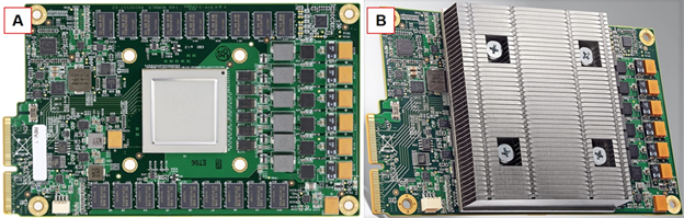
Google has never said how many TPUs it connects to one server motherboard before overloading the motherboard’s processing capabilities or its PCI-Express throughput. Coprocessors require a lot of care and attention from their host processor, in the form of task setup and teardown and managing data transfer bandwidth in and out of each TPU. Coprocessors only do one thing, but they are designed to do that one thing very well.
Google has designed its TPU2 for use in a four-rack stamp, which Google calls a pod. A stamp is a standard rack configuration (from half-rack to many racks) for a related set of workloads. Stamps help make purchase, installation, and deployment easier and less costly for large datacenter owners. For example, Microsoft’s Azure Stack standard half-rack will be a stamp.
The four-rack stamp size is mostly due to the copper cable types Google is using and the maximum copper run lengths for full-speed operation. The figure below shows the high-level organization of the stamp.
The first thing we noticed is that Google connects each TPU2 board to one server processor board via two cables. It could be that Google connected each TPU2 board to two different processor boards, but it is unlikely that even Google would want to mess with the installation, programming, and scheduling complexity for that topology. It is much simpler if there is a one-to-one connection between a server board and a TPU2 board.
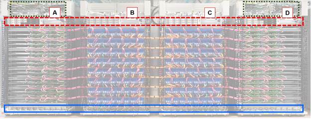
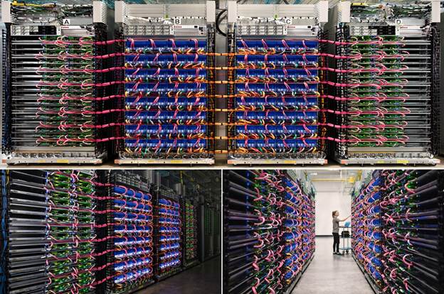
Google showed three different photos of its TPU2 stamps, and the configuration and wiring look the same for all three photos. Garish color coding of the TPU2 cabling helps a lot for this comparison.
Google posted a top view of the TPU2 board and a close-up of the board’s front-panel connectors. Each of the four TPU2 board quadrants shares board power distribution. We believe that four TPU2 board quadrants also share network connections via a simple network switch. It looks like each board quadrant is a separate subsystem and the four subsystems are not otherwise connected to each other on the board.
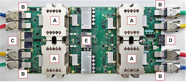
The front panel connections look like a QSFP network connectors flanked by four square cross-section connectors that I have not seen before. The IBM BlueLink specification defines eight 200 Gb/sec signal lanes in each direction (16 lanes total) for a minimal 25 GB/s configuration (called a “sub-link”). Google is a member of OpenCAPI and a founding member of the OpenPowerFoundation, so BlueLink makes sense.
The two connectors in the center of the front of the board look like QSFP-style connectors with copper twisted-pair bundles, and not fiber. That gives two choices – either 10 Gb/sec Ethernet or 100 Gb/sec Intel Omni-Path Architecture (OPA). Two 100 Gbps OPA links can be combined for an aggregate bi-directional bandwidth of 25 GB/s, which matches BlueLink speeds, so we think it is Omni-Path.
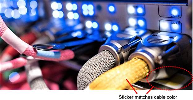
None of these copper cables, BlueLink or OPA, can be run much over 3 meters or 10 feet at maximum signal rate. That binds the interconnect topology linking CPU and TPU2 boards together by a 3m physical spanning distance. Google uses color coded cables; my guess is that makes it easier to assemble without cabling mistakes. See the sticker matching the cable color under the front-most connector in the figure above. We believe that color coding is a sign that Google plans larger scale deployments of these TPU2 stamps.
The white cables are most likely a 1 Gb/sec Ethernet system management network. We do not see a way that Google can connect the management network to the TPU2 boards in the photos. But, based on the routing of the white cables, we do assume that Google connected the management network to the processor boards from the rear. Perhaps the processor boards manage and assess health of the TPU2 boards through their OPA connections.
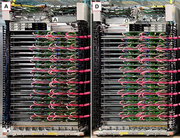
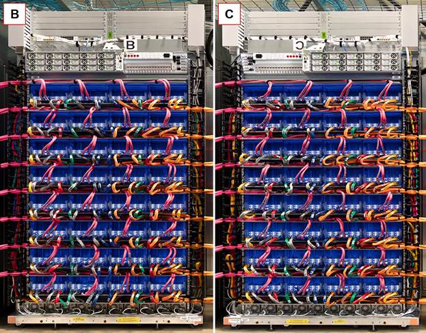
Google’s TPU2 rack stamp has bilateral symmetry. In the figure below we flipped processor rack D to compare it with processor rack A. These two racks are identical but mirrored images of each other. The figure after that, it is obvious that racks B and C are also mirror images of each other.
There is not enough wiring visible in Google’s photos to determine the exact interconnect topology, but it does look like a some kind of hyper-mesh interconnect.
We believe the CPU boards are standard Intel Xeon dual-socket motherboards that fit Google’s 1.5-inch server form factor units. They are a current generation board, given that they have OPA, they may be Skylake boards (see power consumption discussion below). We believe they are dual-socket boards simply because I have not heard that a lot of single-socket boards are shipping through any part of Intel’s supply chain yet. This may change as new market entrants such as AMD with “Naples” Epyc X86 server chips and Qualcomm with Centriq ARM server chips emphasize single-socket configurations.
We believe that Google connected each CPU board to exactly one TPU2 board using both OPA cables to achieve 25 GB/s aggregate bandwidth. This one-to-one connectivity answers a key question for TPU2 – Google designed the TPU2 stamp with a 2:1 ratio of TPU2 chips to Xeon sockets. That is, four TPU2 chips for every dual-socket Xeon server.
This tight coupling of TPU2 accelerators to processors is much different than the 4:1 to 6:1 ratios typical for GPU accelerators in deep learning training tasks. The low 2:1 ratio suggests that Google kept the design philosophy used in the original TPU: “the TPU is closer in spirit to an FPU (floating-point unit) coprocessor than it is to a GPU.” The processor is still doing a lot of work in Google’s TPU2 architecture, but it is offloading all its matrix math to the TPU2.
We cannot see any storage in the TPU2 stamp. Presumably that is what large bundle of blue fiber cables in the overhead chase is for in the figure below. The datacenter network connects to the CPU boards, there are no fiber cables routed to racks B and C and there are no network connections on the TPU2 boards.

There are 32 compute units per rack, whether TPU2 or CPU. There are therefore 64 CPU boards and 64 TPU boards in each stamp, totaling 128 CPU chips and 256 TPU2 chips.
Google says that its TRC contains 1,000 TPU2 chips, but that is rounding down slightly. Four stamps contain 1,024 TPU2 chips. Four stamps are therefore the lower bound for how many TPU2 chips Google has already deployed. Three (possibly four) stamps are visible in the photos they published during Google I/O.
It is not clear how pairs of processors and TPU2 chips federate across a stamp so that TPU2 chips can effectively share data across the links in a hyper-mesh. We are nearly certain that the TRC cannot span a single task across more than one of the four stamps (256 TPU2 chips). The original TPU was a simple coprocessor, so the processor handled all data traffic. In this architecture, processors access data from remote storage across a datacenter network.
The stamp memory model is also not described. Can TPU2 chips use remote direct memory access (RDMA) across OPA to load their own data from memory on the processor boards? It seems likely. It also seems likely that the processor boards might do the same across the stamp, creating a large shared memory pool. That shared memory pool would not be as fast as the memory pool in Hewlett Packard Enterprise’s Machine shared memory system prototype, but with 25 GB/s links it won’t be slow and it might still be quite large, in the two digit terabyte range (16 GB per DIMM with eight DIMMs per processor, two processors per board, and 64 boards yields 16 TB of memory).
We speculate that scheduling a task which requires more than one TPU2 on a stamp would look something like this:
- The processor pool should have a map of the stamp’s hyper-mesh topology and which TPU2 chips are available to run tasks.
- Groups of processors might federate to program each TPU2 to explicitly connect a mesh between connected TPU2 chips.
- Each processor board loads data and instructions onto the four TPU2 chips on its paired TPU2 board, including flow control for a mesh interconnect.
- The processors synchronize booting a task across interconnected TPU2 chips.
- When a task completes, the processors collect the resulting data from the TPU2 chips (that data might already be in the global memory pool via RDMA) and flag the TPU2 chips as being available for another task.
This method has the advantage that the TPU2 chips don’t need to understand multitasking, virtualization, or multitenancy – the processors have the task of handling all of that across the stamp.
It also means that if Google ever offers a Cloud TPU instance as part of its Google Cloud Platform custom machine type IaaS, the instance will have to include both processors and TPU2 chips.
It is also not clear that workloads can be scaled across stamps and retain the low latencies and high throughput of the hyper-mesh. While researchers may have access to some of the 1,024 TPU2 chips via TRC, scaling workloads across stamps looks like a challenge. Researchers will probably have the ability to connect clusters of up to 256 TPU2 chips – which is impressive enough, given cloud GPU connectivity is currently expanding up to 32 interconnected devices (via Microsoft’s Project Olympus HGX-1 design).
Google’s first generation TPU consumed 40 watts at load while performing 16-bit integer matrix multiplies at a rate of 23 TOPS. Google doubled that operational speed to 45 TFLOPS for TPU2 while increasing the computational complexity by upgrading to 16-bit floating point operations. A rough rule of thumb says that is at least two doublings of power consumption – TPU2 must consume at least 160 watts if it does nothing else other than double the speed and move to FP16. The heat sink size hints at much higher power consumption, somewhere above 200 watts.
The TPU2 board has huge heat sinks sitting on top of the TPU2 chips. They are the tallest air-cooled heat sinks I have seen in many years. They have internal sealed-loop liquid circulation. In the figure below, we compare the TPU2 heat sinks to the largest comparable heat sinks we have seen over the past few months.
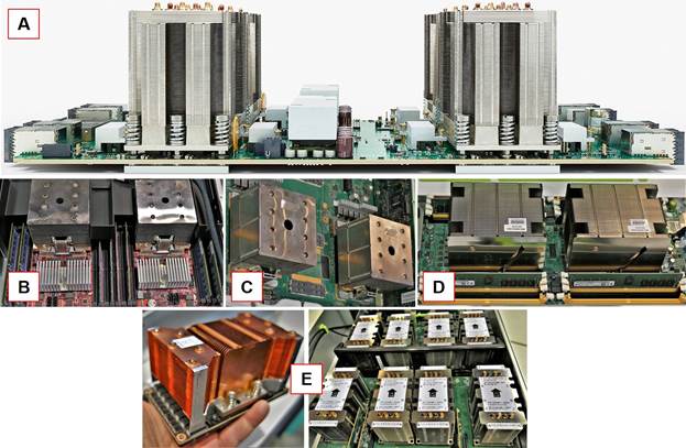
The size of these heat sinks screams “over 200W each.” It is easy to see that they are much larger than the 40 watt heat sink on the original TPU. These heat sinks fill two Google vertical 1.5-inch Google form factor units, so they are almost three inches tall. (Google rack unit height is 1.5 inches, a little shorter than the industry standard 1.75-inch U-height).
It is a good bet that there is more memory per TPU2 chip as well, which contributes to the increased throughput and adds to power consumption.
Also, Google moved from PCI-Express powering single TPU chips – the PCI-Express slot supplies power to the TPU card – to a quad TPU2 board design shared dual OPA ports and switch, plus two dedicated BlueLink ports per TPU2 chip. Both OPA and BlueLink add to the TPU2 board level power consumption.
Google’s Open Compute Project rack spec donations show 6 kilowatt, 12kilowatt, and 20 kilowatt power delivery profiles; the 20 kilowatt power distribution enables 90 watt CPU processor sockets. We guess that with Skylake generation Xeon processors and the TPU2 chips handling most of the compute load, racks A and D probably use 20 kilowatt power supplies.
Racks B and C are a different story. Power delivery of 30 kilowatts would enable 200 watt power delivery to each TPU2 socket; 36 kilowatt per rack would enable 250 watt power delivery to each TPU2 socket. 36 kilowatts is a common high performance computing power delivery spec. We believe 250 watt power consumption per chip is also the only reason Google would pay for those huge TPU2 heat sinks shown in above. Power delivery for a single TPU2 stamp is therefore probably in the 100 kilowatts to 112 kilowatts range and is probably closer to the higher number.
That means the TRC consumes nearly half a megawatt of power while operating at full capacity. While four stamps is expensive to deploy for research, it is a one-time capital expense and doesn’t occupy a lot of data center space. However, half a megawatt of electricity is a lot of operating expense to fund on a continuing basis for academic research, even for a company of Google’s size. If the TRC is still operating in a year, that will indicate Google is serious about finding new use cases for its TPU2.
A TPU2 stamp contains 256 TPU2 chips. At 45 teraflops per TPU2 chip, each stamp produces an aggregate 11.5 petaflops of deep learning accelerator performance. That is impressive, even if it does turn out to be peak FP16 performance. Deep learning training often requires higher precision, so FP32 matrix multiply performance is likely to be one quarter of FP16 performance, or about 2.9 petaflops per stamp and 11.5 FP32 petaflops for the TRC as a whole.
At peak performance, this implies 100 gigaflops to 115 gigaflops per watt for FP16 operations across the stamp (not including CPU performance contributions or storage located outside of the stamp).
It will be possible to calculate the Xeon processor’s FP16 and FP32 performance and add that to the aggregate performance per watt after Intel discloses dual-socket Skylake generation Xeon core count and power consumption configurations.
There is not enough information yet about Google’s TPU2 stamp behavior to reliably compare it to merchant accelerator products like Nvidia’s new “Volta” generation. The architectures are simply too different to compare without benchmarking both architectures on the same task. Comparing peak FP16 performance is like comparing the performance of two PCs with different processor, memory, storage, and graphics options based solely on the frequency of the processor.
That said, we believe the real contest is not at the chip level. The challenge is scaling out compute accelerators to exascale proportions. Nvidia is taking its first steps with NVLink and pursuing greater accelerator independence from the processor. Nvidia is growing its software infrastructure and workload base up from single GPUs to clusters of GPUs.
Google chose to scale out its original TPU as a coprocessor directly linked to a processor. The TPU2 can also scale out as a direct 2:1 accelerator for processors. However, the TPU2 hyper-mesh programming model doesn’t appear to have a workload that can scale well. Yet. Google is looking for third-party help to find workloads that scale with TPU2 architecture.
Paul Teich is an incorrigible technologist and a Principal Analyst at TIRIAS Research, covering clouds, data analysis, the Internet of Things and at-scale user experience. He is also a contributor toForbes/Tech. Paul was previously CTO and Senior Analyst for Moor Insights & Strategy. For three decades Teich immersed himself in IT design, development and marketing, including two decades at AMD in product marketing and management roles, finishing as a Marketing Fellow. Paul holds 12 US patents and earned a BSCS from Texas A&M and an MS in Technology Commercialization from the University of Texas’ McCombs School.

Google Cloud Mainstreams AI With Vertex Platform
For the past several years, tech giants have been trying to make artificial intelligence in its many guises HPC, data analytics, and other advanced workloads more available and easier to use for enterprises. Traditional OEMs such as Hewlett Packard Enterprise, Dell Technologies, and Lenovo are using a combination of hardware, …
Anthropic Fires Off Performance And Price Salvos In AI War
It is a strange time in the generative AI revolution, with things changing on so many vectors so quickly it is hard to figure out what all of this hardware and software and people-hours costs and what it might be worth when it comes to transforming, well, just about everything. …
Chiplet Cloud Can Bring The Cost Of LLMs Way Down
If Nvidia and AMD are licking their lips thinking about all of the GPUs they can sell to the hyperscalers and cloud builders to support their huge aspirations in generative AI – particularly when it comes to the OpenAI GPT large language model that is the centerpiece of all of …
Outstanding analysis Paul!
I don’t think google is aiming this architecture with its topology for their cloud business (it would be too energy inefficient) it’s more likely they are aiming this hyper mesh architecture with for researchers only in order to improve the scalability of neural networks.
I think a cloud service based on TPU2 (or a subsequent generation) is a long-term goal, but first Google has to learn to schedule deep learning tasks that 1) span boards and 2) span stamps.
Interesting article but disagree that half a megawatt requires significant opex. US prices per MWh available from eia.gov, $30 seems a fair number (probably high for Google), 4,380 MWh needed per year, gives me about $131K/year for this rack. Small change vs the R&D and capex.
Thanks for the article. Guess we will have wait until the next version of the TPUs before Google ahres the details.
Thanks for reading!
I think that once the folks kicking the tires of TFRC start publishing we’ll learn a lot more. We’ll see.
So this means in 12-18 months time then. Also would be interesting to know if these TPU-2 chips are still done on 28nm or if they have moved up a note now.
Why do you assume that QSFP is OPA? QSFP with copper cables is widely used for 100Gbps Ethernet (which would fit well in Google’s wider network) or 100Gbps Infiniband as well. OPA would strongly tie this design to Intel CPUs only, which seems unlikely for Google (though possible).
I agree that the processor boards are likely connected to Google’s data center fabric via Ethernet, but InfiniBand requires expensive add-in NICs and it is likely that Skylake server SKUs have built-in OPA. I’m going to say that built-in wins here, Google is much more likely to use OPA on the TPU2 side. https://www.nextplatform.com/2015/05/26/intel-lets-slip-broadwell-skylake-xeon-chip-specs/
Will Google build a version of the TPU2 board that has BlueLink/OpenCAPI connectivity to the processor board? We’ll have to wait for POWER9 launch and Zaius processor boards to find out… https://www.nextplatform.com/2016/10/17/opening-server-bus-coherent-acceleration/
so the effiency is somewhere around 200 watt for ~45 TFLOPS of FP16, making them less efficient than Volta. what is the benefit? production costs?
I try to use real world workloads when comparing products, and in this case Google hasn’t provided any, nor have they provided enough information to make educated guesses. Comparing peak raw throughput is never a good idea, especially when most of the industry is assuming that Google’s peak raw throughput number for TPU2 is FP16 – Google has not actually said so.
Porter’s forces model (originally there were five) describes the basics of business competition, and one of the big ‘aha’ moments in the model is noticing the impact of a few large suppliers. In this case the large suppliers are Intel for its Xeon processors and NVIDIA for state-of-the-art GPUs. So, if Google invests $100 million in TPU development and buys 1 million GPUs from NVIDIA each year, then break-even for creating internal competition to an external supplier would be negotiating a $100 discount per GPU. $100 per GPU is probably on the order of a 5% discount for the high-end GPUs that Google buys and at the volumes that Google buys them. So, if their actual costs are lower, their volume is higher, or their negotiated discount is higher, it was well worth the investment.
But don’t try this at home, this can only be attempted by SaaS vendors who control their own deep learning framework, as Google does with TensorFlow. Microsoft Azure is going in the same direction with their custom ‘Catapult’ FPGA-enabled NICs, but Microsoft has CNTK. AWS offers GPU and FPGA enabled instances, but hasn’t yet stepped to the plate for custom acceleration because they haven’t created or adopted a deep learning framework that they control.
BTW, this is likely the same reason that Google is also investing in OpenPOWER – to address Intel Xeon pricing. Unlike deep learning accelerators, there is no point in Google trying to develop a processor alternative in-house. Best bet for Google in the processor market is to try to act as a king-maker and promote an external competitor to Intel.
The benefit is 200W gives you 180tops, not 45
Never mind. I understand where you are getting that number now
Linkedin analyst had Google was #1 on where engineers wanted to work.
The TensorFlow framework as over 58k stars on GitHub. More than any other and is newer.
Google has 7 products with over 1 billion active users. Google getting more data than any other company from those services.
Then we have the silicon with the TPUs.
Earlier this week Google AlphaGo beat the best player in the world. Go can NOT be solved by brute force but takes some “intuition” to win. Go was not thought to be beat for another 6 – 10 years depending who you talk to .
Might be a bold statement to make but looks to me that the AI space has already been won just many do not realize it.
I found this sentence confusing: “The IBM BlueLink specification defines eight 200 Gb/sec signal lanes in each direction (16 lanes total) for a minimal 25 GB/s configuration”
Further reading leads me to believe that each lane is 25 Gb/sec, so 8 lanes is an aggregate of 200 Gb/sec or 25 GB/s.