

Chip maker Intel takes Moore’s Law very seriously, and not just because one of its founders observed the consistent rate at which the price of a transistor scales down with each tweak in manufacturing. Moore’s Law is not just personal with Intel. It is business because Intel is a chip maker first and a chip designer second, and that is how it has been able to take over the desktops and datacenters of the world.
Last month, the top brass in Intel’s chip manufacturing operations vigorously defended Moore’s Law, contending that not only was the two year cadence of transistor price/performance improvements still on track, but that its processes, at any given node, were superior to those of its competitors. And as such, Intel issued a rallying cry for the industry to return to a more rigorous definition of transistor scaling that had been deployed in the past so processes can be more accurately compared across chip makers.
Ever since Dennard scaling ran out of gas for Intel and all other chip makers and the entire industry had to shift to making processors with ever-increasing parallelism rather than ones with ever-faster clock speeds, Intel shifted to a two-step method of improving the performance of its processors and keeping its revenues and profits growing more or less in lock step for its Data Center Group. The tick was a shrink to a new manufacturing process, which allows for more transistors to be put on a die and more chips to be put on a wafer, lowering the cost of each transistor and chip; although each process shrink costs increasingly more money to develop and put into production, Intel’s the net gain in density allows for price/performance improvements and Intel’s increasing chip volumes allow for it to get more revenues and profits. The tock was a shift to a new architecture, with improvements in instructions per clock and often increasing L2 and L3 cache as well as widening vector processors and other things to boost performance. This way, Intel is only making one kind of major change at a time, rather than two. This lowers risk and has allowed it to provide consistent performance improvements every two years.
To be fair, there was always two phases of ticking and tocking going on at Intel, which lowered its risks in the server business even further. The PC client chips, the Atom and Core families, got the new processes way ahead of the Xeon and then Xeon Phi families. The ramp in a new process was perfected on the client chips, which have much higher volumes and which therefore allow for the production ramp to scale up faster than it would if it had debuted on server chips, which have much lower volumes, first. This strategy has worked brilliantly for Intel, and no other chip maker has been able to do this. Qualcomm, which has a volume ARM client chip business, is trying to replicate this two phase client-server chip ramp strategy by adding its Centriq line of ARM server chips this year. Microsoft has committed to use the Centriq chips on its Azure cloud and has ported Windows Server to these and other ARM server chips for internal use only.
Back in July 2015, Intel conceded that Moore’s Law improvements were slowing, but in the past two years it has created a set of technologies that it calls hyperscaling (not to be confused with the term used to describe the scale of the infrastructure at Google, Facebook, Amazon, Microsoft, Baidu, Tencent, Alibaba, and China Mobile) that allow it to keep the Moore’s Law improvements in price/performance in transistors on a two-year track. The new argument that Intel has put out essentially comes to this: The rate of change in improvements are still on the two year curve, but it takes three steps to make the improvements and it takes longer than two years to make the jumps sometimes. We call this tick-tock-clock because the changes in process and microarchitecture continue as before, but the microarchitecture tweak now includes speedups in transistor speeds (within the same power envelope) as well as a follow-on boost in transistor performance. Like this, as Mark Bohr, an Intel Senior Fellow and director of process architecture and integration, explained in his presentation during the Technology and Manufacturing Day that Intel hosted:
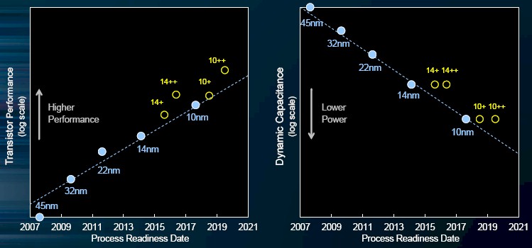
As you can see, there is not just a 14 nanometer or 10 nanometer process any more, but actually three different iterations for each process shrink. So, technically, the Intel method for making chips is actually something more like (tick-clock)(tick-tock-clock)(tick-clock with a dash of tock maybe), but that just doesn’t roll off the tongue the same way as tick-tock-clock. Just because Intel manufacturing creates a process does not mean that the product groups have to use it in production for their chips, and Intel was not specific that the base 14 nanometer process was used for the “Broadwell” Xeon E5 v4 chips launched in March 2016 or that the 14+ process would be used for the future “Skylake” Xeon chips due later this summer, but let’s assume for argument’s sake that this is the case and that the Broadwell Xeons had the initial tick for the 14 nanometer process and the two follow-ons have the 14+ and 14++ processes will be used for Skylake and “Kaby Lake” Xeons. Here then is what the historical and future process trends for client and server chips at Intel looks like:
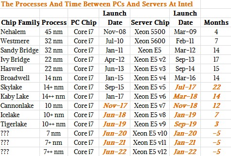
Moore’s Law is interesting and all, but ultimately what matters to datacenters is that there is not too much of a lag between the process and microarchitecture improvements embodied in the client chips, as expressed by the top-end Core i7s in the table above, and the standard Xeon E5 parts for two-socket servers, which have been the workhorses of the datacenter for more than two decades now. And as you can see, the gap for the Skylake generation of chips got very long indeed if Intel actually ships in volume the Skylake Xeons in July of this year. (We put in July not because we know, but because we know it is not impending even if it is looming, and we are well aware that Google is already selling Skylake Xeon E5 instances on its Cloud Platform public cloud. We don’t count such early shipments for this table. There are always early adopter customers who pay a premium, and it used to be selected HPC shops but now it is a handful of HPC and hyperscaler organizations that help Intel ramp and move themselves to the front of the line.) Cannonlake is supposed to ship in clients by November of this year, basically alongside the new Kaby Lakes, and if Intel had stuck to an 18 month separation that could mean Xeon E5 v7 server chips based on Kaby Lake would come in July 2018 and on Cannonlake in in May 2019. We originally said that Intel could shorten the gaps between Cores and Xeons, and this is apparently what will happen, and then some.
In a conference call this week going over the financial results for Intel’s first quarter of 2017, Robert Swan, Intel’s new chief financial officer, said that Data Center Group would be the first of its groups to use its 7 nanometer processes and would be a fast follower on 10 nanometer processes. So, the chart above has been tweaked in real time by us to not just show the gap between Xeons and Cores closing, but reversing. The dates shown above in orange are straight up guesses to make a Xeon and a Core in every process and to get Xeons ahead of Cores at the first 7 nanometer iteration.
What is important here is that this tick-tock-clock method allows Intel to be more regular in its launches and to get its server product line out to the summer of 2022 on the 7 nanometer processes that it now has in development and that, as Bohr explained, will not require a move from 300 millimeter wafers to 450 millimeter wafers to stay on that Moore’s Law price/performance curve. By the way, that is a two-year acceleration of the Xeon roadmap, which with an 18-month gap with the Cores would have pushed it to the summer of 2024. If you don’t think Intel thinks that ARM and AMD are not competitive threats in the datacenter, think again.
Peering Into 14 Nanometer And 10 Nanometer Processes
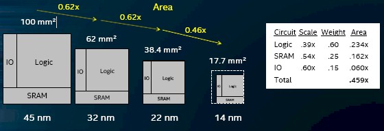
Because the areal density of a chip is so interrelated with the yield on the manufacturing process and thus to the cost and profitability of a chip, Intel spent a lot of time drilling down into the advances it has made in conjunction with the 14 nanometer and 10 nanometer nodes that allow it to shrink the areal density well beyond what you would expect with a plain vanilla Moore’s Law shrink in transistor sizes. The chart below, provided by Ruth Brain, Intel Fellow and director of interconnect technology and integration in the Technology and Manufacturing Group, is a blended average of area shrinkages for Core and Xeon chips implemented in each process:
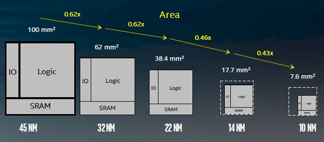
With normal areal density improvements, you would expect that a chip with 100 square millimeters of area implemented in 45 nanometer processes would shrink to 23.8 square millimeters at 14 nanometers and 14.8 square millimeters at 10 nanometers. But thanks to the hyperscaling techniques, it has been able to get a 0.46X scaling factor with 14 nanometer processes, down to 17.7 square millimeters, and a 0.43X scaling factor at 10 nanometer processes, pushing that chip down to 7.7 square millimeters. So Intel can cram nearly 13 chips into the same space on a 300 millimeter wafer that one chip back in 2008 used to take.
This is impressive, but this, more than anything else, is what Intel does for a living, and Intel is the best chip maker in the world at this.
Let’s start with the 14 nanometer processes, plural, which Brain described during the Technology and Manufacturing Day. The base 14 nanometer process went into production in 2014, with the follow-on 14+ process coming out in 2015 and the 14++ process in 2016.
In general, Brain said that Intel’s 14 nanometer family was about a factor of 1.3X denser than the 20 nanometer and 14/16 nanometer processes available from competitive fabs such as Taiwan Semiconductor Manufacturing Corp, Globalfoundries, and Samsung, and that its 14 nanometer node had about the same transistor density as the 10 nanometer processes that its competitors were expected to roll out – and Intel was three years ahead of that competition.
![]()
Brain added that the performance of its transistors, in terms of switching speed, was about 20 percent higher than the competition at these respective (and what Intel says are equivalent) process nodes.
To get the hyperscaling effect required to keep on the Moore’s Law curve, Intel has to work on various feature pitches and heights in the circuitry, and here is how these were tweaked moving from the 22 nanometer generation, the first to have FinFET 3D transistors, to the more refined 14 nanometer process:
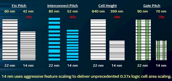
The scaling was different for each feature, and was particularly for the fin, interconnect, and gate pitches on the transistors. If Intel reverts to the traditional way of measuring logic area scaling, as Bohr explained on Technology and Manufacturing Day, then you measure the gate pitch in a transistor and multiply it by a NAND logic circuit’s cell height. (This NAND is not the same NAND we refer to in flash memory, but the way a NAND logic circuit is constructed from the transistors.) If you do that math, then the jump from 45 nanometers to 32 nanometers at Intel yielded a scaling factor of 0.49X, the jump from 32 nanometers to 22 nanometers yielded a 0.45X shrink, and the move from 22 nanometers to the initial 14 nanometer process resulting in a 0.37X scaling.
Here is how Brain stacked up the initial 14 nanometer process, first used with the Broadwell family of Core and Xeon chips as well as the “Knights Landing” Xeon Phi parallel processor:

Intel’s 14 nanometer processes had their first wafer starts at about the same time that the competition rolled out their 20 nanometer processes; the 14 nanometer and 16 nanometer processes from the competition came out about a year later. And, said Brain, intel is ahead on every density metric, regardless of the naming conventions companies use to describe their circuits.
That helps a lot, but performance increases don’t just come from adding more transistors that yield more cores and caches, but also by increasing the raw switching performance of the transistors themselves. Here is how the transistor performance of the three different 14 nanometer flavors stack up at Intel:
![]()
The 14+ process allowed a 12 percent increase in current drive in desktop products introduced in 2015, in Xeon Phi chips in 2016, and in Skylake Xeons coming out this year. With the 14++ process used with the “Kaby Lake” desktop chips as well as in the new Xeon E3 chips that were just launched and in future Xeon E5 processors (there doesn’t look to be an E7 going forward), the drive current is, depending on if you are measuring NMOS or PMOS transistors, boosted by 23 percent or 24 percent compared to the initial 14 nanometer process rolled out by Intel. Brian added that the current 14++ process had greater than 20 percent better current drive than the 14/16 nanometer processes from the competition out there.
The upshot of these drive current enhancements is that the transistor performance can be improved at an annual cadence, like this:
![]()
The cadence allows for the client and server groups at Intel to make use of this transistor performance improvement in a number of ways. In the jump from 14 to 14++ processes, the transistors can run 28 percent faster or run at the same performance but with 52 percent lower active power draw; chip engineers and plot out different SKUs that mix and match the tradeoff between performance and power in between these brackets.
Another key innovation that is driving the hyperscaling embodied in the 14 nanometer processes is self-aligned double and quad patterning, which are etching techniques that provide better geometries for circuit components than standard litho/etch techniques, which Intel contends have yield and performance risks because doing multiple masks when you run the litho/etch cycle twice is a very difficult process to control. The etchings can get miss aligned and the pitches get out of whack, and that means you have to throw away a wafer. This is always a bad thing.
The die scaling for 14 nanometer processes is significant, and we presume that this is actually comparing the 14++ process to the prior processes:
The upshot is that with the 14 nanometer process and related hyperscaling techniques (which are more about geometry and layout of components than transistor size), Intel can get around 1.4X the number of chips per dollar on 300 millimeter wafers. By moving from 300 millimeter wafers to 450 millimeter wafers, the wafers cost 1.6X more, but you can get 2.25X as many chips on the die for – you guessed it – a 1.4X increase in the units per dollar spent. What this means is this: If Intel can stay on 300 millimeter wafers for 7 nanometer processes, it can decide at that point to move to bigger wafers and not have to do a jump to 5 nanometers to lower its costs. The transition to 450 millimeter wafers will be expensive indeed, and such a strategy would not yield increases in performance. But those might not be coming so easily anyway, and if this becomes a price war for compute, Intel has a big gun in its back pocket that it can haul out and, perhaps, its rivals will not be able to afford. (This is a transition that no one can really afford, as such.)
Now, for some show and tell on the 14 nanometer chips, which Intel showed off here:
Look at how clean that FPGA is. It is a tabula rasa, indeed.
Let’s zoom in on the server chip on the bottom left:
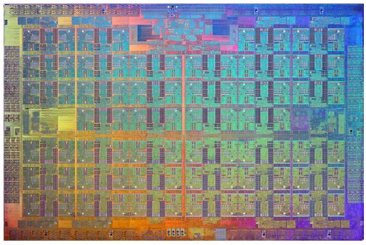
As best we can figure, that is the “Knights Landing” Xeon Phi parallel processor, launched in June 2016, and we counted all 76 of the cores there. In the production machine, because of yield issues on this monstrous processor, which has over 8 billion transistors, Intel only delivers 72 cores on the top bin part. The most common parts have 64 cores, or only 84 percent of those on the die, fired up. So the yields must be kind of challenging.
The Easter egg that Bohr put in his charts is the server chip that is center bottom of the 14 nanometer family. Take a zoom in:

There is a very, very high probability that this is none other than the top-bin 28-core Skylake Xeon processor, unmasked.
Honey, I Shrunk The Chips
While the Xeons are still waiting to get the 14+ process, all eyes are on the 10 nanometer processes that have given Intel a bit of a headache bringing to market because these will be the etchings the future of the Xeon product line from 2019 through 2021
The move to 10 nanometer processes has aggressive hyperscaling on various features, according to Kaizad Mistry, corporate vice president in the Technology and Manufacturing Group and co-director of logic technology development. Here is how the shrinkage looks across different parameters:
With the improved transistor designs, the 10 nanometer processes (due to have wafer starts late this year and coming to market in client PCs in early 2018 we think) will yield a transistor density of 100.8 million transistors per square millimeter (MTr/mm2), compared to 15.3 MTr/mm2 for the 22 nanometer processes and 37.5 MTr/mm2 for the 14 nanometer processes.

In addition, the FinFET fins in the 10 nanometer processes are 25 percent taller and 25 percent skinnier than those used in the 14 nanometer processes, which in turn were about 30 percent taller and skinnier than the initial FinFET fins in the 22 nanometer processes, and this yields higher performance and lower power for the transistors. Adding to this is a the fact that Intel is moving the transistor contact atop the active gate, instead of below it, and that is giving Intel back another 10 percent of the transistor area that can be used to cram more transistors on a die and keep Moore’s Law moving. On top of this, Intel is implementing a single dummy gate architecture for logic cells, instead of the double dummy gates at cell boards, and this is giving back yet more area for useful circuits – somewhere around 20 percent of the effective area, with the most effect on a 2-imput NAND cell and the least on the complex scan flip-flop logic cell. (These are the two circuits that are used to calculate transistor density.) The upshot is that with the 10 nanometer process move and the hyperscaling features mentioned above, Intel can get another 0.37X scaling factor moving from 14 nanometers to 10 nanometers – the same as it got jumping from 22 nanometers to 14 nanometers and better than it has averaged with prior process node jumps.
This provides a 2.7X improvement in transistor density over the course of about three and a half years, and about 2X the density that competitive 10 nanometer processes will be yielding at about the same time, according to Mistry.
As with the 14 nanometer processes, the 10 nanometer ones will sport interim 10+ and 10++ tweaks with increase performance on the transistors. Here is what it is looking like:
![]()
The usual tradeoffs between active power and performance apply, but the initial jump to 10 nanometers yields a 25 percent improvement in transistor performance and the 10++ jump at the end will yield another 15 percent at constant active power. It doesn’t look like the 10+ process will do much here in terms of power efficiency or increased performance, since it logically has to be between these two lines.
The 10 nanometer processes will enter manufacturing in the second half of this year, and is to be used in the “Knights Hill” kicker to the current Knights Landing Xeon Phi and will debut in the “Aurora” supercomputer being made by Intel and Cray for Argonne National Laboratory. If the roadmap scuttlebutt is right, then 10 nanometer processes will be used for the “Cannonlake” Xeons due in 2019 and for two generations, using 10+ and 10++ processes, after that, and that gets us to 2021.


With Sapphire Rapids Launched, Gelsinger Focuses On The Future
Pat Gelsinger returned to Intel as CEO in early 2021, the same year that the company was supposed to launch is much-touted fourth-generation Xeon SP processor, dubbed “Sapphire Rapids.” Almost two years later and after multiple delays, Gelsinger on Tuesday finally was able to take the stage and announce the …
The Pax Chipzilla Is Over, And Intel Can’t Hold Back The Barbarians
It is the nature of big tech companies with near monopolies to start looking a bit like Rome in its Golden Age – the Pax Romana that held from when Augustus Caesar became emperor in 27 BC until Marcus Aurelius died in 180 AD. During these peaceful times, all things …
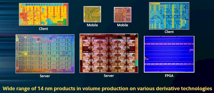
Intel Hopes To Accelerate Datacenter And Edge With A Slew Of Chips
It is hard to say how many Xeon and Xeon SP CPU sales have been obliterated by Nvidia GPUs, but the number is a big one. And that is why Intel finally came around to the idea that GPU compute was not just going to be a niche thing, but …
The second graph doesn’t make much sense since Intel has already announced that they will go a data center first starting at 10nm++ (Icelake).
Fair enough. We updated the table to reflect the latest very thin rumors for Icelake and Tigerlake. We will see what happens.
No, it is datacenter thitd, since before 10nm++ there will be 10nm+ and 10nm.
Thanks for this fascinating article. Intel and the industry in general has an amazing ability to coordinate progress in so many difficult, complex fields so as to produce reliable products within a year or two of the basic research being finalized. Design and manufacture is amazing enough, but how do they test these devices, in a few seconds, at one temperature, and be so sure that they will continue to work for decades at a range of elevated temperatures, over a range of power supply voltages and clock speeds?
Debris from the upper atmosphere cosmic ray collisions rips through these devices all the time, and yet they function reliably with ever fewer electrons per bit. As the features become ever smaller, I wonder how these chips will survive atomic diffusion over the decades to come. If there is a major socio-economic disruption, to the point where Intel and similar companies are unable to continue manufacturing, humanity would be dependent for centuries on the existing stock of CPUs etc. – with the smallest-featured chips failing first. I had some regrets when junking a perfectly functional 350nm Pentium Pro and MB the other day.