

Four years ago, Google started to see the real potential for deploying neural networks to support a large number of new services. During that time it was also clear that, given the existing hardware, if people did voice searches for three minutes per day or dictated to their phone for short periods, Google would have to double the number of datacenters just to run machine learning models.
The need for a new architectural approach was clear, Google distinguished hardware engineer, Norman Jouppi, tells The Next Platform, but it required some radical thinking. As it turns out, that’s exactly what he is known for. One of the chief architects of the MIPS processor, Jouppi has pioneered new technologies in memory systems and is one of the most recognized names in microprocessor design. When he joined Google over three years ago, there were several options on the table for an inference chip to churn services out from models trained on Google’s CPU and GPU hybrid machines for deep learning but ultimately Jouppi says he never excepted to return back to what is essentially a CISC device.
We are, of course, talking about Google’s Tensor Processing Unit (TPU), which has not been described in much detail or benchmarked thoroughly until this week. Today, Google released an exhaustive comparison of the TPU’s performance and efficiencies compared with Haswell CPUs and Nvidia Tesla K80 GPUs. We will cover that in more detail in a separate article so we can devote time to an in-depth exploration of just what’s inside the Google TPU to give it such a leg up on other hardware for deep learning inference. You can take a look at the full paper, which was just released, and read on for what we were able to glean from Jouppi that the paper doesn’t reveal.
Jouppi says that the hardware engineering team did look to FPGAs to solve the problem of cheap, efficient, and high performance inference early on before shifting to a custom ASIC. “The fundamental bargain people make with FPGAs is that they want something that is easy to change but because of the programmability and other hurdles, compared with an ASIC, there ends up being a big difference in performance and performance per watt,” he explains. “The TPU is programmable like a CPU or GPU. It isn’t designed for just one neural network model; it executes CISC instructions on many networks (convolutional, LSTM models, and large, fully connected models). So it is still programmable, but uses a matrix as a primitive instead of a vector or scalar.”
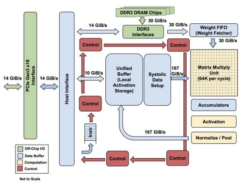
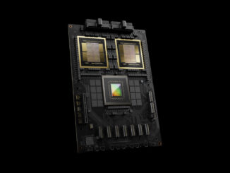
The TPU is not necessarily a complex piece of hardware and looks far more like a signal processing engine for radar applications than a standard X86-derived architecture. It is also “closer in spirit to a floating point unit coprocessor than a GPU,” despite its multitude of matrix multiplication units, Jouppi says, noting that the TPU does not have any stored program; it simply executes instructions sent from the host.
The DRAM on the TPU is operated as one unit in parallel because of the need to fetch so many weights to feed to the matrix multiplication unit (on the order of 64,000 for a sense of throughput). We asked Jouppi how the TPU scales and while it’s not clear what the upper limit is, he says anytime you’re working with an accelerator that has host software there’s going to be a bottleneck. We are still not sure how these are lashed together and to what ceiling, but we can imagine, given the need to have consistent, cheap hardware to back inference at scale, it is probably not an exotic RDMA/NVlink approach or anything in that ballpark.
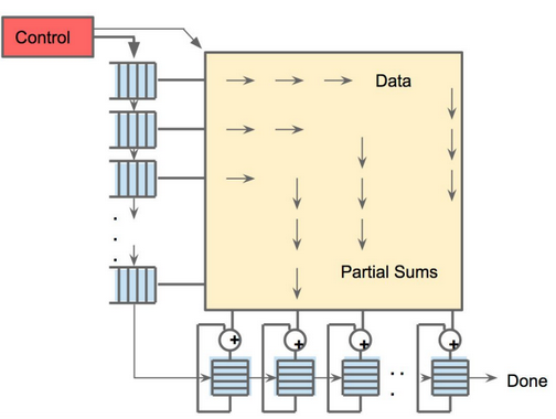
There are two memories for the TPU; an external DRAM that is used for parameters in the model. Those come in, are loaded into the matrix multiply unit from the top. And at the same time, it is possible to load activations (or output from the “neurons”) from the left. Those go into the matrix unit in a systolic manner to generate the matrix multiplies—and it can do 64,000 of these accumulates per cycle.”
It might be easy to say that Google could have deployed some new tricks and technologies to speed the performance and efficiency of the TPU. One obvious choice would be using something like High Bandwidth Memory or Hybrid Memory Cube. However, the problem at Google’s scale is keeping the distributed hardware consistent. “It needs to be distributed—if you do a voice search on your phone in Singapore, it needs to happen in that datacenter—we need something cheap and low power. Going to something like HBM for an inference chip might be a little extreme, but is a different story for training.”
Of course, the true meat of this paper is in the comparisons.
While Google has been thorough in its testing, pitting its TPU against both CPUs and GPUs, given that most of the machine learning customer base (with the notable exception of Facebook) uses CPUs for processing inferences, the comparisons to the Intel “Haswell” Xeon E5 v3 processors is no doubt the one that is most appropriate and this is one that shows without a doubt that the TPU blows away Xeon chips on multiple dimensions when it comes to inference workloads. And that explains why Google went to the trouble of creating its own TPU chip when it would have by far preferred to keep running machine learning inference on its vast X86 server farms.
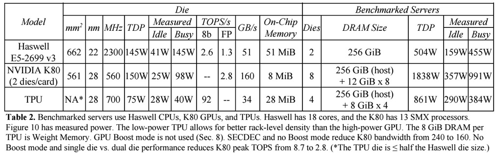
In Google’s tests, a Haswell Xeon E5-2699 v3 processor with 18 cores running at 2.3 GHz using 64-bit floating point math units was able to handle 1.3 Tera Operations Per Second (TOPS) and delivered 51 GB/sec of memory bandwidth; the Haswell chip consumed 145 watts and its system (which had 256 GB of memory) consumed 455 watts when it was busy.
The TPU, by comparison, used 8-bit integer math and access to 256 GB of host memory plus 32 GB of its own memory was able to deliver 34 GB/sec of memory bandwidth on the card and process 92 TOPS – a factor of 71X more throughput on inferences, and in a 384 watt thermal envelope for the server that hosted the TPU.
Google also examined the throughput in inferences per second that the CPUs, GPUs, and TPUs could handle with different inference batch sizes and with a 7 milliseconds.
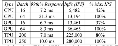 With a small batch size of 16 and a response time near 7 milliseconds for the 99th percentile of transactions, the Haswell CPU delivered 5,482 inferences per second (IPS), which was 42 percent of its maximum throughout (13,194 IPS at a batch size of 64) when response times were allowed to go as long as they wanted and expanded to 21.3 millisecond of the 99th percentile of transactions.The TPU, by contrast, could do batch sizes of 200 and still meet the 7 millisecond ceiling and delivered 225,000 IPS running the inference benchmark, which was 80 percent of its peak performance with a batch size of 250 and the 99th percentile response coming in at 10 milliseconds.
We realize that Google tested with a relatively old Haswell Xeon, and that with Broadwell Xeon E5 v4 processors, the instructions per clock (IPC) of the core went up by around 5 percent due to architectural changes and with the future “Skylake” Xeon E5 v5 processors due this summer, the IPC might rise by 9 percent or even 10 percent if history is any guide. Increase the core count from the 18 with the Haswell to the 28 in the Skylake, and the aggregate throughput of a Xeon on inference might rise by 80 percent. But that does not come close to closing inference gap with the TPU.
Recall again. This is an inference chip, hence the GPU compares we see in the paper are not the knocks against GPUs in general it may seem–they still excel at training models at Google alongside CPUs. The real test for CPU makers (okay, Intel) is to provide something with great inference performance at cost and efficiency figures that can at least come close to a custom ASIC–something most shops can’t do.
“A lot of the architectures were developed a long time ago. Even if you look at AVX extensions for X86—as Moore’s Law scales these have gotten wider but they are still one-dimensional. So when we were looking at FPGAs as one idea and saw that wouldn’t work we started thinking about the amount of silicon we could get out of 28nm—that allows for things that were unheard of back in the day when the vector was a high end machine. Now, we can take it to the next level with a tensor processing unit with the matrices at the heart—it is exciting because we don’t get to change often in this industry…From scalars to vectors, and now to two-dimensional tensors.”
“We did a very fast chip design, it was really quite remarkable. We started shipping the first silicon with no bug fixes or mask changes. Considering we were hiring the team as we were building the chip, then hiring RTL people and rushing to hire design verification people, it was hectic,” Jouppi says.
The paper is being presented by another pioneer in computing–David Patterson, the inventor of RAID disk protection and “father of RISC”… quite a stellar (and large) team on this.

Google Needs Another Database To Attack Oracle, DB2, And SQL Server Directly
Why does Google need another database, and why in particular does it need to introduce a version of PostgreSQL highly tuned for Google’s datacenter-scale disaggregated compute and storage? It is a good question in the wake of the launch of the AlloyDB relational database last week at the Google I/O …
Industry Behemoths Back Intel’s Universal Chiplet Interconnect
When the hyperscalers, the major datacenter compute engine suppliers, and the three remaining foundries with advanced node manufacturing capabilities launch a standard together on Day One, this is an unusual, significant, and pleasant surprise. And this is precisely what has happened with Universal Chiplet Interconnect Express. The PCI-Express interconnect standard …
Hyperscalers Bringing Nvidia’s Grace-Blackwell Superchip To Their Clouds
At his company’s GTC 2024 Technical Conference this week, Nvidia co-founder and chief executive officer Jensen Huang, unveiled the chip maker’s massive Blackwell GPUs and accompanying NVLink networking systems, promising a future where hyperscale cloud providers, HPC centers, and other organizations of size and means can meet the rapidly increasing …
Interesting architecture, but given the massive growth in deep learning (and thus money involved, and thus becomes interesting for big players like Nvidia and Intel), I don’t expect Google to keep using their TPUs, but rather to switch to off-the-shelf FPGAs (like Altera) or ASICs (like Nervana) in the next couple of years, given those could be built on the most advanced process nodes.
TPU is an ASIC (and Nervana is gone with the win..tel). And with the size of Google, the cost of designing ASICs to save power and get the additional benefits of a domain-specific architecture.
I agree. There are several vendors doing custom-ASICs for deep learning. This chip design and capabilities (only 70x over a Xeon) is not impressive. The only impressive part of this story is the capability of doing something from scratch in that amount of time. But I guess, that if you have the $$$ and the resources is not that challenging either. If you follow the architectecture/microarchitecture conferences in the last 5 years, there are far better designs than this one. Not only for inference, but also for training. With an ASIC you should get around three orders of magnitude of improvement.
As I understand it’s part of ongoing R&D, not something they’re going to commercially offer, and should not be judged as such. I’d say a factor 70 over the current top of the line is pretty okay for a first generation of new hardware. I doubt this is the end point, and expect will integrate what they learn while using this into making even more efficient ASICs.
If only Google had the kind of talent that presents at these conferences, or had access to the resulting papers
Give that a Tesla P4 is at least 16x more energy efficient than a K80 (*), it feels disingeneous of google to brag about efficiency when compared to a 5 year old kepler architecture.
*https://devblogs.nvidia.com/parallelforall/new-pascal-gpus-accelerate-inference-in-the-data-center/
The Pascal (derplearn) Teslas have only been officially released a few weeks before the submission deadline of the research paper in question, so expecting to compare to those is just silly.
On the other hand, it is fair to criticize the paper for not comparing (also) against the Maxwell M4/M40, indeed as GM20x are also on 28 nm and have significantly better performance than the K80s (though not more than 1.5-2x), I’d guess.
why? all the software runs right off the bat (plug and play) furthermore other peoples benchmark data was readily available from the get go… as you mention skipping maxwell gen to…
they are obviously wanting to hype their solution by comparing it to ancient hardware, very bad paper.
I agree. This is more a marketing papers and was accepted because was coming from google. They should have done a sound evaluation against contemporary architectures (at the time of the design) and current architectures.
Your document must have been missing the first page, which says “To appear at the 44th International Symposium on Computer Architecture (ISCA), Toronto, Canada, June 26, 2017”. Thus, it is a peer-reviewed scholarly paper that will be presented at a conference that accepts less than 20% of submissions
Not only that it is an unfair comparison toward the Haswell as well why where they using 64bit float on Haswell and 8bit Int on their ASIC. They could have used 8bit int on Haswell as well and probably would have got 8-10x more TOPs. Which would have shrinked their margin to laughable 7 times.
Em, NO. 64 divided by 8 is really 8, butt:
Haswell has very wide FMA vector units. Stunning 32 operations per cycle. (16 MUL + 16 ADD).
But on Integer side there are 2 vector ALU but only one vector MUL unit (which is kind of bad for matrix multiply operations).
So for int8 they can achieve 32 MUL operations + 64 ADD (from which 32 will be utilised).
That means they can achieve 2x better performance in ideal case (no carry logic, no owerflows, no data conversion…)
OK so whats for dinner?? You folks astound me (64 yr old gent) who loves this stuff but was left behind in the race…
If you were to select one solid player who would you put your $ on…
your name has been my laptop’s password for the past two years.
Arguing about exactly which CPU/GPU/FPGA the TPU should be compared with is missing the point — an ASIC (remember what the “AS” stands for?) will always annihilate more general purpose programmable devices because it’s built to do one thing and do it extremely well, and no amount of CPU/GPU/FPGA tweaking will close this gap.
Correct, but an ASIC is expected to get a least 2 or 3 orders of magnitude better than existing more general solutions, and this is not the case neither 🙁 . They only remarkable job here is putting out a chip in production in few months.
Care to give a concrete example of a programmable ASIC product that does what you claim?
Hi David,
With all due respect, Can I ask whether you’re the David Patterson who worked on the TPU project itself and just won a Turing Award?
Hi David,
With all due respect, Can I ask are you the David Patterson who was on the Google TPU team and just won a Turing award?
Hmm, no, I think the 2.8 TOPS for the GPU compared to the 92 TOPS for the TPU using half the power was a big part of the point. But it’s been known for some time that NVIDIA has a card (Tesla P4) that could theoretically provide, when using 8 bit math (like the TPU uses), about 4 times the TOPS while using 1/4th the power as the GPU used in the paper. That gives the TPU only about 4 times the energy efficiency of the P4. That’s not such an annihilation considering the general purpose nature of the GPU. I didn’t read the paper, but I also wonder if TensorRT (or the earlier GPU Inferencing Engine) was used to optimize the network on the GPU. That would provide additional power efficiency for the GPU.
Deep learning is a quickly evolving field and the K80 was already a dinosaur at the time the paper was published. That just reduces the usefulness of the comparisons in the paper. The TPU is still faster, but the amount by which it is faster is wildly different from what’s presented in the paper.
I think NVIDIA might be coming out with their own inferencing ASIC, though.
can not agree more.
P4 is more power and power efficient which minimize the gap of GPU and TPU.
“never excepted” … expected ?
Does anyone know the detail of the systolic architecture?As they decribed,the multiplication array’s scale is 256×256. when the data Bx256 matrix,weights is 256×256 matrix,it will cost B cycles to complete the matrix multiplication:data x weights. It is hard to image how to complete the 256 accumulation in one cycle?
I realize it’s more fun to opine than to actually read the paper, but it says in Section 3:
“The benchmark platforms are server-class computers that were available in 2015 when the TPUs were deployed. This restriction meant that they must include at least SECDED protection of internal SRAM as well as external DRAM memory like the TPU, which excludes some choices such as the Nvidia Maxwell GPU” since it doesn’t provided error protection for on-chip memory
Maybe Mr. Jouppi and the crew could explore the route of designing a SQL Processing Unit, I am sure such a board would save billions CPU’s cycles per day per data center.