

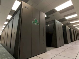
The future “Summit” pre-exascale supercomputer that is being built out in late 2017 and early 2018 for the US Department of Energy for its Oak Ridge National Laboratory looks like a giant cluster of systems that might be used for training neural networks. And that is an extremely convenient development.
More than once during the SC16 supercomputing conference this week in Salt Lake City, the Summit system and its companion “Sierra” system that will be deployed at Lawrence Livermore National Laboratory, were referred to as “AI supercomputers.” This is a reflection of the fact that the national labs around the world are being asked to do machine learning on the same machines that would normally just do simulation and modeling to advance science, not just to advance the art of computation but to make these systems all look more cool and more useful. With pre-exascale machines costing hundreds of millions of dollars, it is important to get the most use out of them as possible.
Considering how long ago the architectures for Summit and Sierra were done, it is perhaps a happy coincidence for IBM, Nvidia, and Mellanox Technologies that a hybrid and hefty combination of CPUs and GPUs has become the preferred node type for training the neural networks that drive machine learning as well being the system architecture of choice for boosting the speed of GPU-accelerated database management systems.
Details of the final Summit and Sierra nodes were divulged at the SC16 conference, and they are interesting in a few ways. And they reflect the fact that any procurement of a supercomputer is done so far in advance that it is hard to predict exactly what configuration of system will come to market years after the funds are allocated in budgets to build machines like Summit and Sierra.
Way back in November 2014, when the CORAL procurements were announced to put three capability-class, pre-exascale systems into Oak Ridge, Lawrence Livermore, and Argonne National Laboratory, the total bill for these three machines was set at $325 million. This included the 180 petaflops “Aurora” supercomputer at Argonne National Laboratory, which is based on Intel’s future “Knights Hill” Xeon Phi processors and its 200 Gb/sec Omni-Path 2 interconnect and storage based on the Lustre parallel file system (also from Intel), all in a projected 13 megawatts of power consumption. Intel is the primary contractor (a first) on Aurora and Cray is the subcontractor actually doing the system integration, with the system being installed in 2018. For the Summit and Sierra systems, which were originally slated to weigh in at 150 petaflops each as a minimum peak performance, the machines are based on a mix of Power9 processors from IBM and Tesla “Volta” GV100 GPU accelerators with 100 Gb/sec InfiniBand EDR networking and storage based on IBM’s GPFS parallel file system, all crammed into a 10 megawatt power envelope.
If you allocated the money for the CORAL contract linearly (which is not necessarily how it was done), then the Aurora machine costs $122 million and the Summit and Sierra machines cost $101.5 million each. And again assuming that linear pricing across architectures, that means Aurora would have a bang for the buck of $677 per teraflops of peak theoretical performance, exactly the same price/performance of the Summit and Sierra machines. The Aurora machine has 20 percent more performance as specified, but consumed 30 percent more watts as estimated in the original RFP, so in a sense it is less power efficient than either Summit or Sierra. It is hard to predict the future, maybe especially with a supercomputer. You might need one to make such simulations. . . .
Pushing The Envelope
The original Summit specification called for the system to be comprised of around 3,400 nodes with more than 40 teraflops of performance using an unspecified combination of Power9 CPUs and Volta GPUs. Some presentations, such as this one we detailed by Nvidia chief technology officer Steve Oberlin from ISC15 comparing the two architectures, had Summit at 3,500 nodes to deliver that performance.
It looks like it is going to take more nodes to get Summit to its performance level, but nowhere near the more than 50,000 “Knights Hill” Xeon Phi nodes that are expected to be ganged up to get Aurora to 180 petaflops. And it looks like Summit will be getting a networking upgrade, too, with Mellanox confirming last week that it would be able to get 200 Gb/sec High Data Rate (HDR) InfiniBand into the field in the middle of next year and shipping in both the Summit and Sierra machines.
We caught wind of the final Summit node configurations at SC16 this week, and here is what they look like:
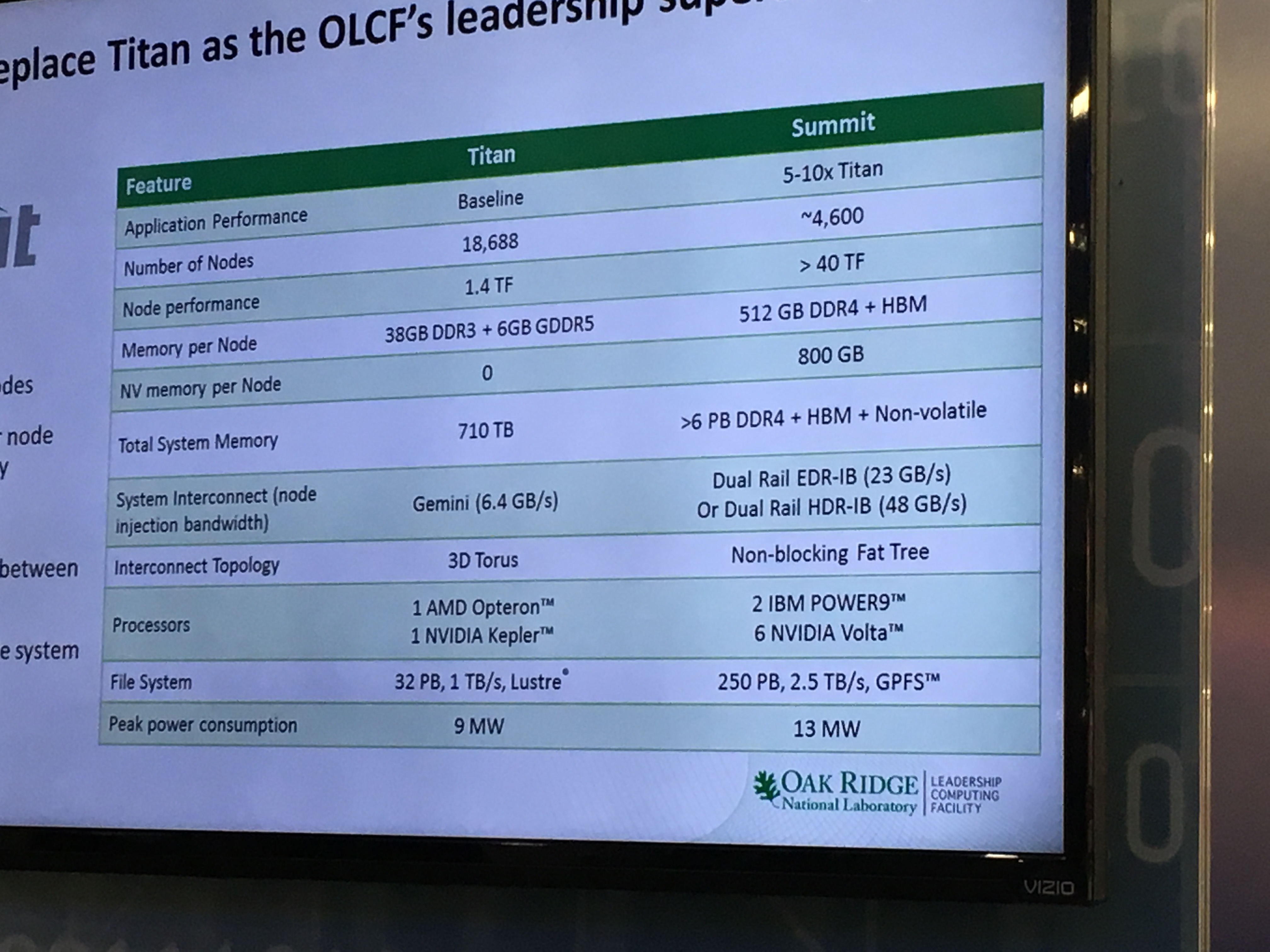
As you can see, the node count for Summit has been boosted to 4,600 total, an increase of 35 percent from the original discussion two years ago about the configuration of the machine.
Oak Ridge confirmed in presentations that each of the Summit nodes will have two Power9 chips and six of the Tesla Volta coprocessors. The Power9 chips have 24 cores each and have a midpoint design clock speed of 4 GHz, just like the Power8 chips; clock speeds can be anywhere from a low of 2.5 GHz to as high as 5 GHz, we reckon, depending on the thermal envelope customers want. Oak Ridge has not talked about what core counts and clock speeds it will use for the Power9 processors in the Summit machines.
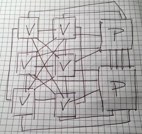
The Power9 chips will have 48 lanes of PCI-Express 4.0 peripheral I/O per socket, for an aggregate of 192 GB/sec of duplex bandwidth, as well as 48 lanes of 25 Gb/sec “Bluelink” connectivity, with an aggregate bandwidth of 300 GB/sec for linking various kinds of accelerators. These Bluelink ports are used to run the NVLink 2.0 protocol that will be supported on the Volta GPUs from Nvidia, and which have about 56 percent more bandwidth than the PCI-Express ports. IBM could support a lot of the SMX2-style, on-motherboard Tesla cards in a system, given all of these Bluelink ports, but remember it needs to allow the Volta accelerators to link to each other over NVLink so they can share memory as well as using NVLink to share memory back with the two Power9 chips.
It will be interesting to see what topology the NVLink network has on the Summit systems and if Volta will support four or eight ports on the die. Obviously, you want as few hops as possible across those six GPUs and between the GPU cluster and the CPU pair. Each Pascal GP100 GPU has four NVLink 1.0 ports on it, and that is not enough to use NVLink to connect four GPUs to each other and to both of the pair of Power8 CPUs at the same time. But if Volta has eight NVLink 2.0 ports, as we have been led to believe it probably will, that really opens up the connectivity for NVLink. You can directly connect each GPU accelerator with each Power9 chip, and still have six ports left over to cross link all of the GPUs to each other. You only need five more NVLink ports to link all of the GPUs to each other in a mesh without having to resort to other kind of switching, and that still leaves an eighth NVLink port leftover. It might look something like this:
Yeah, we still like paper.
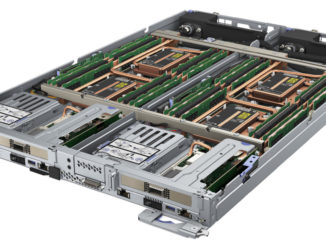
Given that IBM has said that it believes that a ratio of two processors to four GPU accelerators is the sweet spot in the enterprise and that it is trying to keep the form factor of the Power Systems LC HPC-style nodes at a consistent 2U of rack space, it is interesting that IBM is delivering a “Witherspoon” Power Systems LC node that has six Tesla Volta V100 accelerators in it.
We think that IBM and Nvidia are under pressure to make the Summit machine more powerful, and is cramming more GPUs in the nodes and scaling up the number of nodes to make it happen. At 43.5 teraflops peak, the Summit machine at 4,600 nodes would break through 200 petaflops of peak theoretical performance, which would probably put IBM at the top of the Top 500 supercomputer rankings in November 2017 if the machine can be up and running with Linpack by then. This 200 petaflops number is a psychological barrier, not a technical one, but in a Trump Administration, it might be a very important psychological barrier indeed. (China is winning the Petaflops War.)
The original plan called for Summit to be in a 10 megawatt thermal envelope, but that has been boosted by 30 percent to 13 megawatts. Some of that increased power budget could be due to the extra compute capacity, some to extra storage capacity. The original Summit specs called for a 120 PB GPFS file system with 1 TB/sec of bandwidth, but as you can see from the chart above, that file system has grown to 250 PB of capacity with a whopping 2.5 TB/sec of bandwidth. That is 2.1X more capacity and 2.5X more bandwidth, and that is very likely some of the extra power consumption. Ditto for the boosted compute capacity on the larger Summit cluster, and we think IBM and Nvidia might have geared down the Volta GPUs to get better performance per watt in the Summit nodes and boosted the GPU count in the box by 50 percent from four accelerators to six accelerators to scale the performance a bit. (We are admittedly guessing on that. But if IBM and Nvidia are not doing this, the obvious question is: Why not?)
The upshot is that we think Oak Ridge is going to be getting a more capacious Summit machine than it was originally thought possible, and that is a very good thing. IBM, Nvidia, Mellanox, and the Department of Energy might have been hedging their bets on the initial specs, under-promising so they could over-deliver later, and this is understandable given the number of technology transitions that were happening at the same time in the Summit (and therefore Sierra) machines.
The Summit configuration also tells us, perhaps, something about the Volta GPUs, or at least the ones being used inside of Summit.
Way back when, in early 2015, Nvidia said that it would be able to deliver Pascal GPUs with 32 GB of HBM memory on the package that delivered 1 TB/sec of bandwidth into and out of that GPU memory. What really happened was that Nvidia was only able to get 16 GB of memory on the package and only delivered 720 GB/sec of bandwidth with that on-package HBM with the Tesla P100 card. No one is making promises about the amount of GPU memory or bandwidth coming with Volta, as you can see above. What Nvidia has said, way back in 2015, is that the Volta GP100 GPUs would deliver a relative single precision floating general matrix multiply (SGEMM) of 72 gigaflops per watt, compared to 40 SGEMM gigaflops per watt for the Pascal GP100.
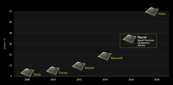
If you use that ratio, and then cut it in half for double precision, then a Volta GPU held at a constant 300 watts (the same as the Pascal package) would have a little over 9.5 teraflops of double precision performance, and four of them would deliver 38.2 teraflops of oomph, the vast majority of the more than 40 teraflops of performance expected in the Summit node. Six GPUs at this performance level would deliver a total of 57.2 teraflops just from the GPUs alone, which no one has promised and that is why we think Nvidia is gearing these Volta GPUs down to maybe 200 watts. If you cut the clocks and therefore the thermals down by 100 watts on each card, you can stay in the same 1,200 watt GPU envelope as four Pascal P100 cards but maybe only cut performance by 20 percent to 25 percent against that 33 percent wattage drop. By moving from four Voltas to six Voltas per node, the HBM memory per node could increase by a lot (100 percent in capacity per card and another 50 percent from having more cards) and the performance per watt and the aggregate performance could be pushed a little further, too. With a geared down Volta card running at 200 watts, you could have a V100 card that deliver 7.6 teraflops at double precision and 38.2 gigaflops per watt compared to something like 38.2 gigaflops per watt for the faster V100 card we theorized above.
For fun, let’s call it 50 teraflops per node in Summit. That is a total of 512 GB of main memory (with 120 GB/sec of bandwidth, according to specs provided by IBM earlier this year), and if Nvidia can reach its original goal of 32 GB of HBM memory per GPU accelerator it hoped to hit with Pascal on the Voltas, that works out to 192 GB of HBM memory with 6 TB/sec of bandwidth. That is a lot more than the 64 GB of HBM memory and aggregate 2.8 TB/sec of GPU memory bandwidth in the current “Minsky” Power Systems LC precursor to the Summit’s Witherspoon node. There is another 800 GB of non-volatile memory in the Summit node, and we are pretty sure it is not Intel’s 3D XPoint memory and we would guess it is flash capacity (probably NVM-Express drives) from Seagate Technologies but Oak Ridge has not said. The math works with this scenario, with 512 GB of DDR4 main memory, a total of 192 GB of HBM memory on the GPUs and 800 GB of flash, across 4,600 nodes that is a total of 6.9 TB of aggregate memory. (By the way, that chart has an error. The “Titan” supercomputer has 32 GB of DDR3 memory plus 6 GB of GDDR5 memory per node to reach a total of 693 TB of aggregate memory.)
At that 50 teraflops of performance per node, which we think is doable if the feeds and speeds for Volta work out, that is a 230 petaflops cluster peak, and if the performance of the Volta GPUs can be pushed to an aggregate of 54.5 teraflops, then we are talking about crossing through 250 petaflops – a quarter of the way to exascale. And this is also a massive machine that could, in theory, run 4,600 neural network training runs side-by-side for machine learning workloads (we are not saying it will), but at the half precision math used in machine learning, that is above an exaflops of aggregate compute capacity.
Boom.
Maybe Summit is not exactly pre-exascale after all.

Lenovo Plays The Long Game, Not The Wrong Game, In Systems
It has been nearly four decades since the Chinese Academy of Sciences handed Liu Chuanzhi and Danny Lui $25,000 to help found Legend, originally a maker of TV sets that, in the wake of the success of the IBM PC and the Apple II computer, decided maybe becoming a maker …
Big Blue Open Sources The Core Inside BlueGene/Q Supercomputers
Earlier this month, we were talking to the James Kulina, the new executive director of the OpenPower Foundation, which is the organization created by IBM and Google back in the summer of 2013 to create a community around the Power architecture. IBM had already open sourced the Power instruction set …
The Financial Longevity That Red Hat Gives IBM
It is hard to imagine, but someday, IBM may not care much about its proprietary System z and Power Systems platforms. Or, more precisely, it may not be able to afford to care the way it has for decades But the good news for Big Blue is that it has …
The slide for Titan is correct. Titan has 18,688 nodes with 32 GB DRAM and 6 GB GDDR for a total of 710 TB.
I am waiting for the two bit floating point FLOPs babble, me.
I think the contract math is off. The Summit and Sierra award was $325M. Argonne (both Aurora and Theta) was a separate $200M contract.
https://www.alcf.anl.gov/articles/introducing-aurora
First exascale? Well… well… if we use single bit precision …