
When IBM started to use the word “open” in conjunction with its Power architecture more than three years with the formation of the OpenPower Foundation three years ago, Big Blue was not confused about what that term meant. If the Power architecture was to survive, it would do so by having open specifications that would allow third parties to not only make peripherals, but also to license the technology and make clones of Power8 or Power9 processors.
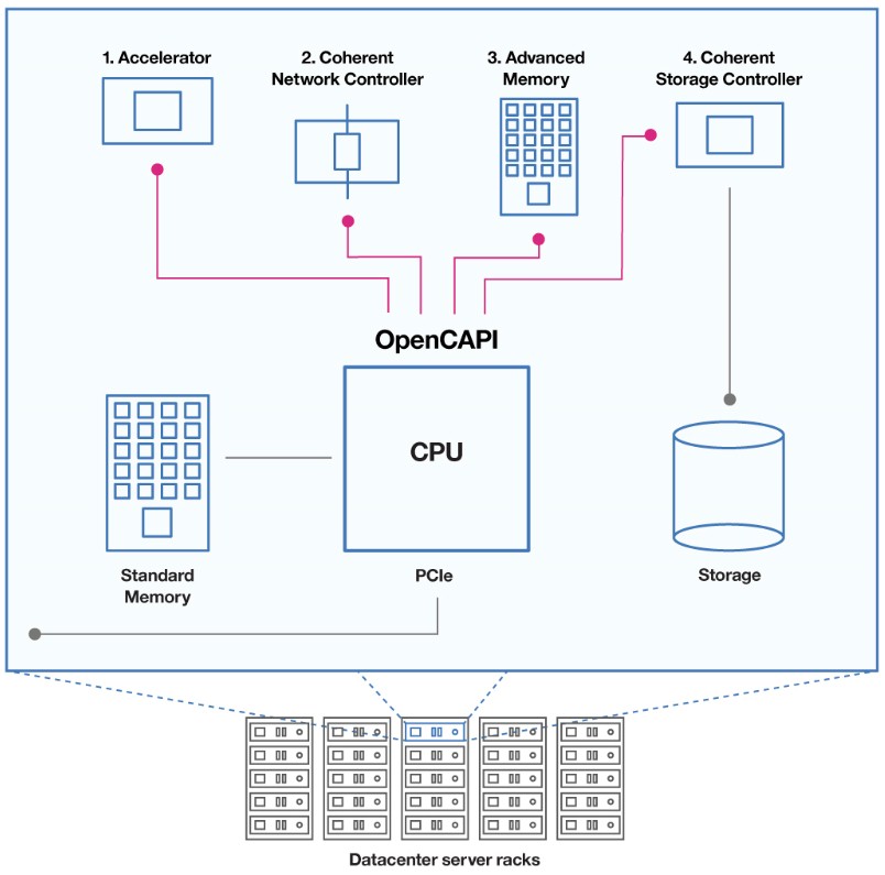
One of the key technologies that IBM wove into the Power8 chip that differentiates it from Xeon, Opteron, ARM, and Sparc processors is the Coherent Accelerator Processor Interface (CAPI), an overlay that uses the PCI-Express bus as a transport but that cuts out all of the overhead needed for supporting legacy I/O and storage devices and allows accelerators hanging off the CAPI protocol to have coherent access to the main memory in the Power8 complex and for the Power8 cores to have access to the memory in the accelerators themselves. (IBM has called the CAPI bus a “hollow core,” which is a good metaphor for how it makes adjunct computing devices look from the point of view of the Power8 processor complex.)
While CAPI has been a key part of IBM’s renewed push in the high performance computing segment, Big Blue wants more from CAPI, so much so that it is willing to create a brand new consortium that will steer its development and foster widespread adoption across all processor makers – including archrival Intel, which has emerged as IBM’s biggest foe in the HPC segment. And OpenCAPI, as the standard that IBM and its systems friends are putting forth is called, seeks to be one of the key protocols for linking components together in systems, along with the CCIX coherent attachment specification announced in May and the Gen-Z storage class memory standard that also debuted last week.
“What is going on here is that we are re-architecting the system,” Brad McCredie, the former president of the OpenPower Foundation and an IBM Fellow and vice president of development in IBM’s Power Systems division, tells The Next Platform. “No matter how you slice it, the processor is not improving cost/performance at the incredible rate and pace that it had in the past. And yet there is still this ever-growing demand for more and more compute capability, driven by these new workloads of artificial intelligence as well as simulation and analytics, there is this huge appetite to still produce more advanced systems. Less and less value is being driven by CPUs and more and more is being generated by accelerators, new memory technologies, and lots of crazy innovations that are attaching to processors. The value is shifting around, and in order to have the ability to mix and match technologies, we are going to need standards and Google, Hewlett Packard Enterprise, and Dell EMC see this very plainly.”
McCredie is referring to IBM’s peers in the formation of the OpenCAPI consortium, who were joined by networker Mellanox Technologies, memory maker Micron Technology, GPU accelerator maker Nvidia, and FPGA maker Xilinx in lining up behind CAPI as a key in-system protocol for linking accelerators and memory of all kinds into the processing complex inside of a system node.
There is a certain amount of confusion about what CCIX, Gen-Z, and OpenCAPI are attempting to do for hybrid systems, and McCredie offered his view on what it all means and how they all fit together, much as some of the top engineers at HPE and Dell did when discussing the Gen-Z protocol with us last week. There seems to be agreement that these standards bodies and their protocols for lashing different things together in systems will be designed to work together, but clear boundaries have yet to be drawn, and frankly, markets will decide – as they always do – what protocols are used where, and how. From his perspective, Gen-Z protocols will be used over various kinds of switched and fabric interconnects, starting with Ethernet, primarily to link various kinds of compute elements, including processors, FPGAs, GPUs, and such, to various kinds of storage class memories that are pooled at the rack level. But OpenCAPI will be concerned primarily with attaching various kinds of compute to each other and to network and storage devices that have a need for coherent access to memory across a hybrid compute complex. (Or, if need be, a monolithic one just made up of processors.)
“Gen-Z’s primary focus is a routable, rack-level interconnect to give access to large pools of memory, storage, or accelerator resources,” says McCredie. “Think of this as a bus that is highly optimized for talking outside of the node at the rack level. OpenCAPI is optimized for inside the node, and it is trying to deal with the fact that we have I/O buses that have one-tenth the bandwidth of main storage buses. With OpenCAPI, I/O bandwidth can be proportional to main store bandwidth, and with very low 300 nanosecond to 400 nanosecond latencies, you can put storage devices out there, or big pools of GPU or FPGA accelerators and let them have access to main store and just communicate to it seamlessly. OpenCAPI is a ground-up design that enables extreme bandwidth that is on par with main memory bandwidth. CCIX is taking a very similar approach, but it is evolving over preexisting standards, like IBM did by having the original CAPI run on top of the PCI-Express 3.0 bus. We are very supporting of CCIX and we think we need to keep moving that standard forward as well. But we also believe there is a need to build on fresh ground for ultimate performance and lowest latency.”
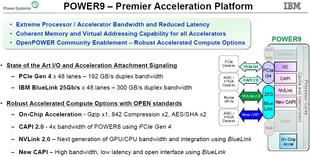
The initial CAPI ports on IBM’s Power8 processors used the on-chip PCI-Express 3.0 controllers as the transport layer for the minimalist coherency protocol it developed to link accelerators and network cards to the Power8 processing complex. With the Power9 chip due in the second half of next year, there will be a slew of different interconnect ports available to linking the processor to other devices. An updated CAPI 2.0 protocol will run atop PCI-Express 4.0 links, which will have twice the bandwidth of the PCI-Express 3.0 ports. That is 16 GT/sec instead of 8 GT/sec, which equates to 31.5 GB/sec of bandwidth in an x16 slot compared to 15.75 GB/sec for a PCI-Express 3.0 slot. So this upgraded CAPI will be no slouch when it comes to bandwidth, at least at peak bandwidth. (Sustained will probably be a lot lower because of peripheral driver and operating system overhead.)
But with New CAPI, as the OpenCAPI port was called when the Power9 chip was unveiled in April at the OpenPower Summit and then talked about in greater detail at the Hot Chips conference in August, IBM it etching new “BlueLink” 25 Gb/sec ports on the chip specifically for coupling accelerators, network adapters, and various memories more tightly to the Power9 chip than was possible with the prior CAPI 1.0 and CAPI 2.0 protocols over PCI-Express 3.0 and 4.0, respectively. It is interesting to note that these same 25 Gb/sec BlueLink ports on the Power9 chip will be able to run the updated NVLink 2.0 protocol from Nvidia. NVLink provides high bandwidth, coherent memory addressing across teams of Tesla GPUs, with NVLink 1.0 supported in the current “Pascal” Tesla P100s and the faster NVLink 2.0 coming with the “Volta” Tesla V100s die next year.
The combination of Power9 and Tesla V100s is the computing foundation of the US Department of Energy’s “Summit” and “Sierra” supercomputers, and from the looks of things, hyperscalers like Google might be interested in similar hybrid machines for its machine learning training. On the Power9 chips aimed at scale-out, two-socket servers, the chips have 48 lanes of PCI-Express 4.0 peripheral I/O per socket, for an aggregate of 192 GB/sec of duplex bandwidth. In addition to this, the base Power9 chip will support 48 lanes of 25 Gb/sec BlueLink bandwidth per socket for other connectivity, with an aggregate bandwidth of 300 GB/sec across those lanes. On the larger scale-up Power9 chips, these 25 Gb/sec BlueLink ports are used to do NUMA communications across four-node clusters; the Power9 chip has separate 16 Gb/sec links to hook four socket modules together gluelessly. So it looks like only the scale-out Power9 chips – the ones that Google and Rackspace Hosting are interested in for their “Zaius” server – will be the ones supporting the BlueLink ports and the OpenCAPI protocol on top of them.
Unless, of course, other processor makers adopt OpenCAPI and either run it on their own communications circuits or license the BlueLink ports from Big Blue. Neither is unreasonable, and the former especially so given that both 100 Gb/sec Ethernet transports and 100 Gb/sec InfiniBand transports are both using 25 Gb/sec signaling now. (This is one reason why the Gen-Z storage class memory interconnect is running first atop Ethernet, although it is not limited to that.) IBM has intentionally separated the OpenCAPI consortium from the OpenPower Foundation so those supporting OpenCAPI don’t have to be part of the Power architecture community.
“We are creating a completely open spec, and everybody is invited, including Intel, to come participate in our spec,” says McCredie, who adds that IBM is perfectly happy to license its BlueLink ports and any microcode and circuitry relating to CAPI 1.0, CAPI 2.0, or OpenCAPI (which is CAPI 3.0) to any company that is interested. (An open specification does not mean open source, of course.) Those who join the OpenCAPI consortium will get an FPGA implementation of the receiver for the OpenCAPI protocol for free, which will allow makers of accelerators, network cards, and storage devices to add OpenCAPI ports on their devices so they can talk to processors and other accelerators that have OpenCAPI ports.
The interesting bit will be when other processor and accelerator makers step up to do target OpenCAPI ports on their devices, not just receivers. IBM is running the NVLink 2.0 protocol over its BlueLink ports, and there is no reason that anyone – AMD with its Zen Opteron and K12 ARM chips, Intel with Xeon and Xeon Phi chips, and a slew of ARM server chip makers – can’t add 25G ports and run OpenCAPI or NVLink on them.
In a way, any processor maker could get a lot of the benefits of the Power9 architecture through OpenCAPI, and while IBM is not begging them to, they would be kind of foolish not to. It is not like IBM and Intel have not cooperated on interconnects and protocols before – both made InfiniBand come into being by merging warring protocols together in 1999, and thought then that the PCI bus had run out of gas. This time, they might be right, or more accurately, that the time has come to start with a clean slate and reuse signaling pins and communications PHYs on chips in many different ways. The PCI-Express stack is a limiter in terms of latency, bandwidth, and coherence. This is why Google and Rackspace are putting OpenCAPI ports on their co-developed Power9 system, and why Xilinx will add them to its FPGAs, Mellanox to its 200 Gb/sec InfiniBand cards, and Micron to its flash and 3D XPoint storage.
We think there will be bridging between OpenCAPI and Gen-Z interconnects and devices, too, much as Ethernet and InfiniBand networks can bridge between each other and, if need be, encapsulate the traffic of each other. Time will tell.

He Who Can Pay Top Dollar For HBM Memory Controls AI Training
What is the most important factor that will drive the Nvidia datacenter GPU accelerator juggernaut in 2024? Is it the forthcoming “Blackwell” B100 architecture, which we are certain will offer a leap in performance over the current “Hopper” H100 and its fat memory younger sibling, the H200? No. Is it …

Who Will Build Europe’s First Exascale Supercomputer – And With What, And Why?
Exascale supercomputing is just as important to Europe as it is to the United States and China, but each of these geopolitical regions on Earth has its own way of developing architectures, funding their development and production, and figuring out where the best HPC centers are to host such machines …
Datacenter Infrastructure Report Card, Q3 2023
It is hard to keep a model of datacenter infrastructure spending in your head at the same time you want to look at trends in cloud and on-premises spending as well as keep score among the key IT suppliers to figure out who is winning and who is losing. And …
This is cool. IBM, as usual, disrupting the market with innovation. Intel as usual will get the benefits
You might need to make a chart that explains the similarities and the differences between all of these new technologies.