
Pattern analytics, deep learning, and machine learning have fueled a rapid rise in interest in GPU computing, in addition to GPU computing applications in high performance computing (HPC) and cloud-based data analytics.
As a high profile example, Facebook recently contributed its “Big Sur” design to the Open Compute Project (OCP), for use specifically in training neural networks and implementing artificial intelligence (AI) at scale. Facebook’s announcement of Big Sur says “Big Sur was built with the Nvidia Tesla M40 in mind but is qualified to support a wide range of PCI-e cards,” pointing out how pervasive Nvidia’s Tesla platform has become for AI research.
Big Sur is a 4U high chassis housing a two-processor (2P) board connected to a daughter card featuring eight full-height double-width PCIe Gen3 x16 300W accelerator card slots intended to house GPU or other PCIe-based compute accelerators. The processor board and daughter card are linked via one PCIe Gen3 x16 slot in the initial implementation. On the daughter card the x16 link is connected to two PLX PCIe switches, each connected to four of the accelerator PCIe slots and also connect to chassis’ network interfaces. Big Sur is a useful baseline to demonstrate why Nvidia’s new “Pascal” Tesla P100 accelerator and the DGX-1 server it has created itself to help customers get up to speed with the Tesla P100 are so important to HPC and pattern analytics.
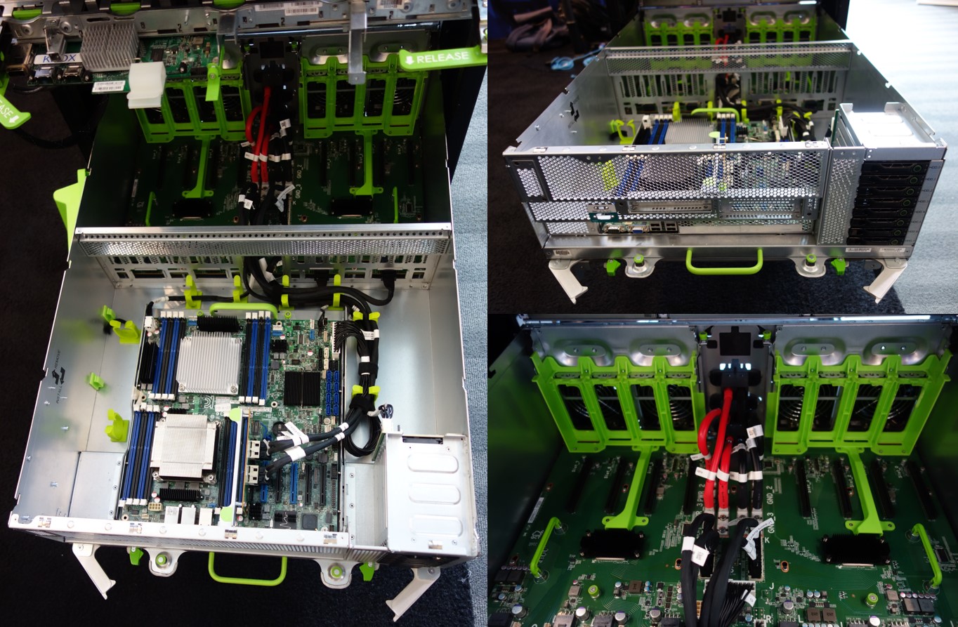
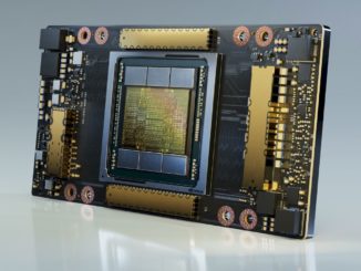
Nvidia Tesla P100 Compute Accelerator
Nvidia claims a number of design innovations in the Tesla P100 accelerator and the DGX-1 system that will increase the performance significantly over other HPC platforms, including:
- The Pascal GPU architecture
- The 16 nanometer FinFET process technology
- A new multi-chip package and high-bandwidth memory
- An enhanced platform interconnect
We separately drilled down into the Pascal GP100 GPU and the Tesla P100 accelerator to give our sense of the importance of the new architecture that Nvidia has debuted, and we also covered the DGX-1 system from Nvidia and talked to one of the first users of the Pascal cards, the Swiss National Supercomputing Center. This is intended to be a complementary analysis that focuses on other aspects of the architecture and the systems that will be using the initial Pascal cards.
Pascal GPU architecture. Nvidia, like all high tech companies, likes to position each new generation of its architecture as transformative, disruptive, and so forth. However, most new processing architectures are little more than evolutions of the previous architecture with an ever increasing emphasis put on power consumption. Nvidia’s architects, on the other hand, chose to increase focus on increased performance in the Pascal GPU architecture, which lead to an increased design complexity, transistor count, and die size of the “data center” version of Pascal. With over 15 billion transistors and a die size of 610 mm^2, this first Pascal GPU is one of the largest processors ever manufactured, and the largest so far in a 16 nanometer FinFET process.
The Pascal GPU implements a scalable compute pipeline. Nvidia organizes their CUDA cores into Streaming Multiprocessors, or SMs, which makes it easy for software developers to code and debug parallel processing resources at manageable scale. Pascal’s 32-bit single precision floating point (FP32) core design supports performing two simultaneous half precision floating point operations (FP16) at the same clock speed as one FP32 operation, using the same compute path. Pascal implements FP32 and double precision floating point (FP64) units in a 2:1 ratio. So, in the time one FP64 operation can be executed, the Pascal architecture can execute four simultaneous FP16 operations. However, only one type of FP instruction – FP16, FP32, or FP64 – may be executed simultaneously in within a single Pascal SM.
Note that Nvidia’s FP16 compute format is fully compliant with IEEE 754-2008, using round-to-nearest-even for all arithmetic. FP16 fully supports subnormal values and they run at the same speed as normalized values.
Also new to the Pascal architecture is unified memory across CPU and GPU physical and virtual memory. A 49-bit virtual address space enables GPU and CPU memory to exist in the same address space while a hardware “page migration engine” globally manages page faults across the unified memory space.
Nvidia also added “compute preemption” to the Pascal architecture – which is a fundamental enabling feature for an operating system or virtual machine to control task execution on Pascal GPUs. Compute preemption coupled with unified memory across CPUs and GPUs will enable Pascal generation GPUs to look and act like a virtualized, composable pool of physical compute resources. The result is that HPC customers can start talking about GPUs in the context of sharable cloud resources, just like CPUs. This will have a huge impact from a software development point of view.
Advanced process technology. Increasing the transistor budget beyond previous generations required the latest process technology to provide any hope of being able to manage the power requirements and obtain a profitably high yield such an ambitious design. To accomplish this, Nvidia transitioned from 28 nanometer planar transistors on its previous generation (the Maxwell GM200 for the Tesla GPUs ) to 16 nanometer 3D FinFET transistors, which significantly reduces leakage power, and skipped a process generation from Taiwan Semiconductor Manufacturing Corp to reduce to die size as much as possible. Pascal’s SM contains 64 CUDA cores, and there are 56 SMs enabled on a Pascal GP100 GPU (the simulated die plot below, provided by Nvidia, shows 60 SMs). The extra SMs allow Nvidia to disable any SMs that do not function properly and still yield a complete part with 56 SMs. This is the same technique used to increase processor yields due to cache block failures by implementing redundant blocks, and Nvidia has used the technique for many years in its GPU designs. Even with 56 SMs, each Tesla P100 has a total of 3,584 CUDA cores.
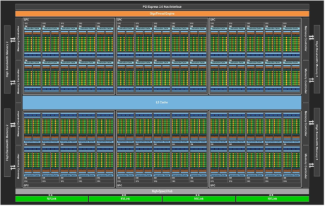
Multi-chip packaging. The Tesla P100 accelerator has a single Pascal GP100 GPU and uses TSMC’s multi-chip packaging, called Chip on Wafer on Substrate (or CoWoS). Nvidia says the Tesla P100 with CoWoS will be in volume production in the third quarter of 2016. Along with the GPU, the CoWoS packaging includes DRAM directly on the substrate. CoWoS implements four second-generation High Bandwidth Memory (HBM) stacks from Samsung, with four 8 Gbit dies for 16 GB of combined on-module physical memory space. Two stacks are located on either side of the huge Pascal die.
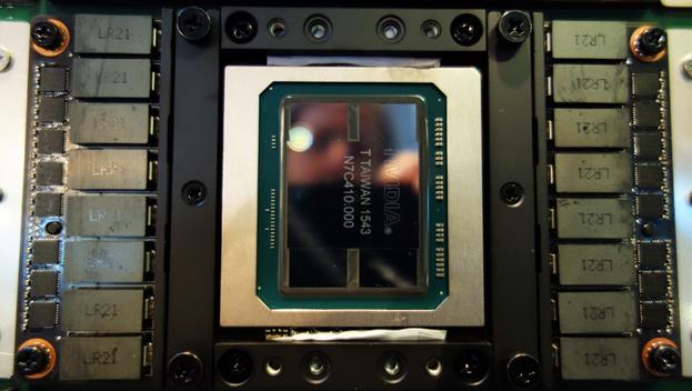
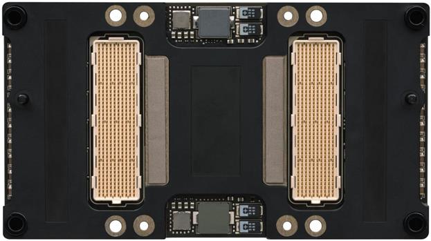
- Vastly increase the number of signal pins to support four NVLink connections instead of only 16 PCIe Gen3 lanes
- Lower the profile of the host chassis
- Supply 300W of power through the motherboard instead of via separate “over the top” wires for power delivery
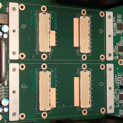
- The P100 module assumes the cost of the 300W power transfer to the CoWoS package via the large, dedicated power management chips (PMICs, shown in the photo)
- No over the top power supply enables use of mechanically simple large passive heat sinks for both the CoWoS package and the PMICs
Air cooling these 300W modules at 35°C ambient temperature is a significant feat of design.
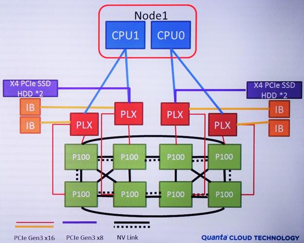
New Package interconnects. Nvidia is moving from third-generation PCI-Express (PCIe Gen3) to its own NVLink interconnect architecture. There are four NVLink x8 links on each P100 module. The P100 also implements an entirely separate PCIe Gen3 x16 interface, which makes it easy to connect four of the DGX-1’s P100 modules to four PCIe Gen3 switches on the GPU board, which in turn connect with the DGX-1 processor board through four PCIe Gen3 x8 connectors. All of these lanes are mapped onto two large connectors on the bottom of the P100 module.
- Memory bandwidth between GPU and its local memory – HBM2 enables a big leap in memory performance, the P100 has 2.5X the memory bandwidth of Nvidia’s own M40 card
- Link bandwidth between GPU modules or between the CPU chipset and GPU card – P100 has 33 percent more effective bandwidth per NVLink connection than the M40 has via PCIe Gen3 x16
- Number of links between GPUs or from GPU to the CPU chipset – GPU cards typically have one PCIe Gen3 x16 link to a PCIe switch or the CPU chipset, where the P100 enables much more flexible interconnect topologies via four independent links that can be ganged if needed
Here’s how Nvidia’s new P100 module stacks up against Nvidia’s classic server add-in boards:
| P100 | M40 | P100 / M40 | K80 | M4 | |
| Double Precision (FP64) TFLOPS* | 5.3 | 0.21 | 26.5x | 2.91 | 0.07 |
| Single Precision (FP32) TFLOPS* | 10.6 | 7.0 | 1.5x | 8.73 | 2.2 |
| Half Precision (FP16) TFLOPS* | 21.2 | N/A | — | N/A | N/A |
| Memory Bandwidth GB/s | 720 | 288 | 2.5x | 480 | 88 |
| NVLink Bandwidth** Peak GB/s | 20 | 16 | 1.25x | 16 | 16 |
| NVLink Bandwidth** Effective GB/s | 16 | 12 | 1.33x | 12 | 12 |
| Number of Links | 5 | 1 | 4x | 1 | 1 |
| Aggregate Link Bandwidth, Effective Bidirectional GB/s | 152 | 24 | 6.33x | 24 | 24 |
| Add-in Card Height | N/A | Full | — | Full | Low |
| Add-in Card Width | N/A | Double | — | Double | Single |
| Power Consumption (Watts) | 300 | 250 | 1.2x | 300 | 50-75 |
* Teraflops – one million million (1012) floating-point operations per second
** Each direction of a bidirectional link
Nvidia says its P100 module is in production now and will ship to hyperscale (cloud) and DGX-1 customers for the rest of this year, and that the P100 module will be available through OEMs in the first quarter of 2017.
Nvidia DGX-1 Server
Nvidia’s DGX-1 server is intended as a full-configured developer system for deep learning applications that can be used by anyone from enterprise users just starting to work with deep learning concepts to supercomputing datacenters working on advanced algorithms. Quanta Cloud Technologies (QCT) was Nvidia’s system development partner and will sell their own version of the system – the QuantaPlex T21W-3U. The substantive difference between the two are:
| Nvidia DGX-1 | QCT QuantaPlex T21W-3U | |
| Faceplate | Fabulous | Vanity-free |
| Availability | Orders now, shipments in US start in Q2, other regions shortly thereafter | Late Q3 or early Q4 for hyperscale customers |
| Pricing | $129,000 | To be announced |
| Software | Complete Nvidia deep learning development stack | None, installed by direct customers, resellers & integrators |
| Support | Hardware and software, see here | Hardware-only |
For the rest of this discussion, we will refer to the two systems’ hardware interchangeably.
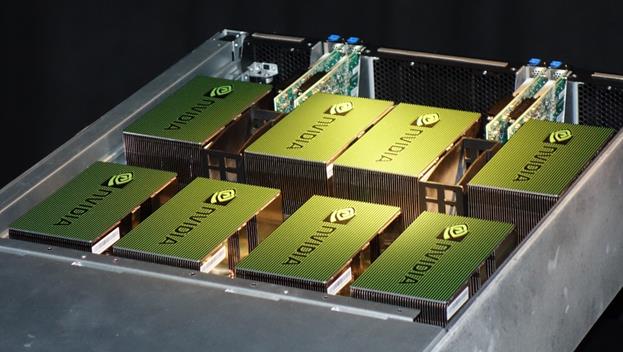
- Chassis: 3U 19-inch rack form factor
- Power Consumption: 3200 Watts at 35°C maximum ambient air temperature
- CPU Board: Dual 16-core Intel Xeon E5-2698v4 CPUs running at 2.3 GHz with up to 512 GB 2133 MHz DDR4 LRDIMMs
- GPU Board: eight Nvidia P100 modules connected via NVLink though two PLX PCIe switches in a flexible hypercube configuration
- Network: Dual 10 GbE or quad InfiniBand EDR 100Gbit channels
- OS: Ubuntu Server Linux OS DGX-1 Recommended GPU Driver
- Turnkey Software: includes major deep learning frameworks, Nvidia Deep Learning SDK, DIGITS GPU training system, drivers, and CUDA
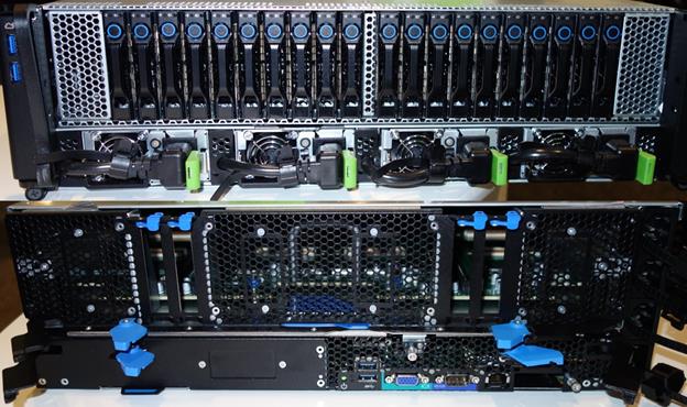
The GPU board with P100 heat sinks is for all intents and purpsoes a 2U system. However, the GPU board is large enough that there is not enough space in the front of the chassis for the 2P server node that controls the GPUs; the 2P CPU board is housed in a separate 1U chassis underneath the 2U GPU chassis and the remaining volume in the 2U GPU chassis is used for storage drives. An enterprising customer or system integrator might disaggregate the two chassis by running the PCIe link between them using an optical link, for example. Disaggregation would allow workloads to optimize the CPU board to balance the compute load but at the expense of extending PCIe between chassis.
The CPU board is designed to meet one of the OCP standard form factors and implements 16 DDR4 DIMM slots with a maximum of 32 GB per DIMM. This initial CPU board may be overbuilt for some customers’ needs and the nice architectural partitioning of the 2P CPU board via the PCIe Gen3 x8 slots will make it easy for system designers and customers to substitute other CPU boards in the future, perhaps to target specific or different machine learning and AI workloads. That might mean a single socket CPU board, perhaps using Xeon D, ARM or OpenPower CPU, or eventually a Xeon processor that integrates an FPGA for additional acceleration. Another option for disaggregation might be to implement shared memory through somewhat slower but more flexible RDMA over Converged Ethernet (RoCE) or InfiniBand’s native RDMA capabilities.
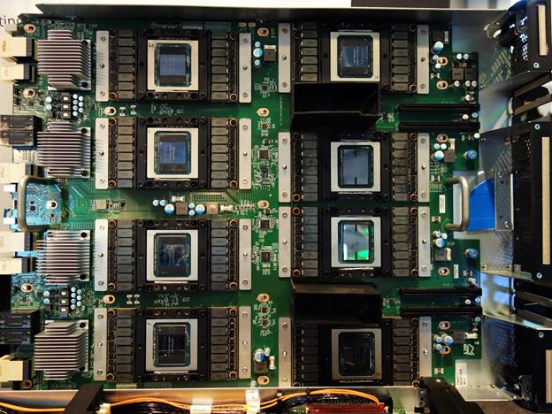
Directly comparing the Facebook contributed OCP Big Sur design to Nvidia’s DGX-1 at a high level:
| Quanta Rackgo X Big Sur | Nvidia DGX-1 / QCT T21W-3U | |
| System | ||
| Rack Height | 4U | 3U |
| Power Consumption | Unstated but comparable given listed components | 3200W |
| Drives | 8x 2.5-inch hot-plug SATA | 12x 2.5-inch hot-plug SAS/SATA
8x 2.5-inch hot-plug NVMe SSD |
| CPU Motherboard | ||
| CPU Sockets | 2 | 2 |
| CPU DIMM Slots | 16 | 16 |
| Accelerator Board Interface | 1x PCIe Gen3 x16 | 4x PCIe Gen3 x8 |
| Accelerator Board | ||
| PCIe Switches | 2 | 4 |
| Number of Accelerators | 8 | 8 |
| Accelerator Card/Module | ||
| Interconnect | PCIe Gen3 x16 via one slot | 4x NVLink via two sockets |
| Format | Full height, double width card | P100 modules |
| Power Consumption | 300W | 300W |
DGX-1 is 25 percent shorter than Big Sur and contains a lot more drive capacity and raw GPU compute power. The DGX-1’s P100 GPU modules are more interconnected (with the ability to tune the connection topology) and have higher throughput than the Big Sur accelerator card slots. DGX-1 is clearly an evolution of the Big Sur design and should easily beat a Big Sur loaded with Nvidia’s M40 or K80 cards at pretty much any GPU-based compute task. While Nvidia is marketing DGX-1 for deep learning, it is simply a beast of a GPU computing system. Period.
It would be fairly easy to swap out the CPU board or simply design in an alternate CPU complex in either design. Which, as it turns out, is what OpenPower is doing with both add-in cards and P100 modules.
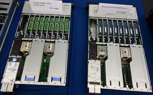
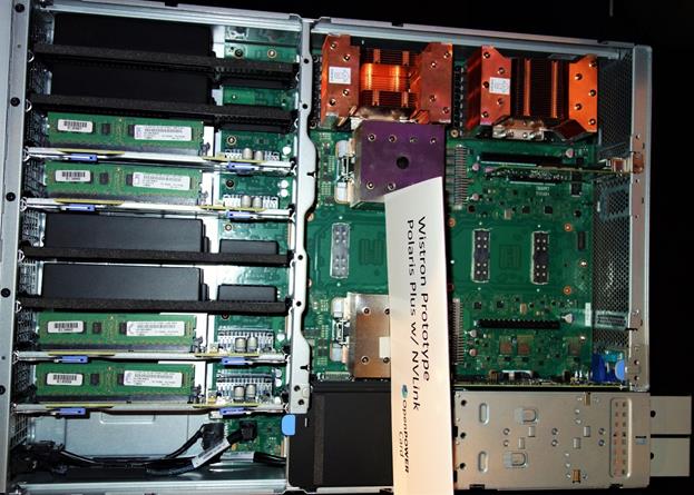
The second annual OpenPower Summit was held concurrently with Nvidia GTC. Two prototype, second generation OpenPower HPC servers with NVLink were on display, one from Wistron (Polar Plus) and another from Zoom (Redpower P210).
These 2U prototypes include two Power8 processors, each with four memory mezzanine cards. There are four P100 modules on the same motherboard as the CPUs; the P100 modules are fully interconnected with each other, and two of the P100 modules each link directly to a Power8 CPU. Each of the Power8 CPUs connects to four memory mezzanine cards, each card hosts four DIMMs, so there are potentially 32 DIMM slots in the front of the chassis.
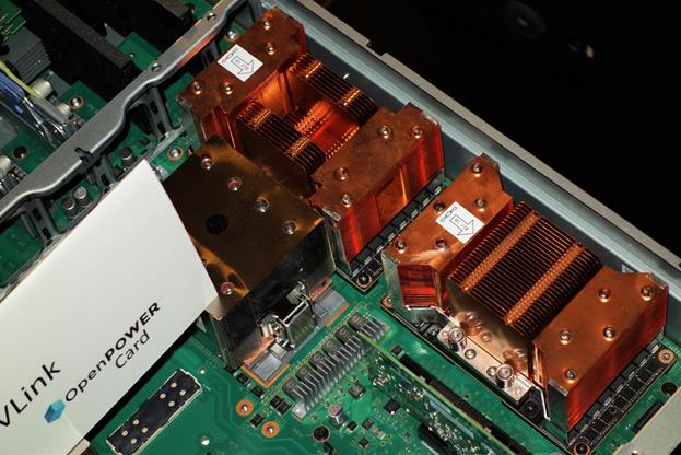
Nvidia’s DGX-1 display system showed different passive heat sinks than the Wistron display system. Except for the Nvidia system’s branded overlay, both sets of heat sinks look production-ready.
The OpenPower ecosystem has been focused on HPC and GPU acceleration since its inception. Nvidia’s P100 module offers OpenPower members a means to move a little faster than most of the more independent x86 HPC vendors.
Conclusion
We believe that Facebook has contributed Big Sur to OCP on the cusp of PCIe-based GPU compute cards becoming irrelevant to the HPC market. One reason Facebook would do this might be to try to boost the volume of the Big Sur platform to lower Facebook’s prices and eke out a little more total cost of ownership advantage for Big Sur as Pascal-based platforms such as DGX-1 move into the high end of the market. Nvidia’s DGX-1 and QCT’s QuantaPlex T21W-3U are not just functionally equivalent to Big Sur, they are superior to Big Sur in every technical respect – they are smaller, faster, and consume comparable power.
While Nvidia’s pricing for the P100 module will keep it at the high end of the market for at least a few quarters, Nvidia is likely to develop smaller derivatives of the initial monster Pascal die (along with new system designs), manufacturing efficiencies will reduce the cost of CoWoS modules, and then falling prices for the P100 and its derivatives will move the capability down-market. Nvidia already has another unannounced GPU accelerator, presumably based on the Pascal architecture, being used on the Drive PX2 for automotive applications. This can be seen on the back side of the DRIVE PX2 board.

Paul Teich is an incorrigible technologist and a principal analyst at TIRIAS Research, covering clouds, data analysis, the Internet of Things and at-scale user experience. He is also a contributor to Forbes/Tech. Paul was previously CTO and senior analyst for Moor Insights & Strategy. For three decades Teich immersed himself in IT design, development, and marketing, including two decades at AMD in product marketing and management roles, finishing as a Marketing Fellow. Paul holds 12 US patents and earned a BSCS from Texas A&M and an MS in Technology Commercialization from the University of Texas McCombs School.



I don’t think this industry shares this vision at all. For the same reason why they are sceptical of having a single supplier in the CPU market they will be sceptical of having a single source of accelerated compute as well. Also nVidia has the same issue as Intel they just can’t get their power density down. On the low end. ASICS, DSP and FPGAs simply will win on the Perf/W
“Nvidia says its P100 module is in production now and will ship to hyperscale (cloud) and DGX-1 customers for the rest of this year, and that the P100 module will be available through OEMs in the first quarter of 2017.”
So how many of these units have actually shipped so far? Was this a “paper launch” with a handful of HPC customers getting some units to test or are they actually shipping in real volume?
I hope Nvidia have Cloud service we can use/ Rent
1. With Tesla P100 to make it stronger and faster
2. Without Tesla P100, so many more people can use the AI without investing it.
Rent maybe can use some option. by computing power or by time or by instance.