
The Power9 processor that IBM is working on in conjunction with hyperscale and HPC customers could be the most important chip that Big Blue has brought to market since the Power4 processor back in 2001. That was another world, back then, with the dot-com boom having gone bust and enterprises looking for a less expensive but beefy NUMA server on which to run big databases and transaction processing systems.
The world that the Power9 processor will enter in 2017 is radically changed. A two-socket system has more compute, memory, and I/O capacity and bandwidth than those behemoths from a decade and a half ago delivered, and while NUMA systems are still important, distributed architectures now rule the datacenter for most workloads, and fat nodes comprised of a mix of processors and accelerators, rather than big CPU-only NUMA clusters, are becoming more common as companies try to create flexible and yet powerful compute complexes to address a wide variety of workloads.
As the variety and complexity of Intel’s own processor roadmap attests, the age of general purpose computing, where a few CPU SKUs covered the bases, is pretty much over. The modern system, as we have discussed numerous times here at The Next Platform, is going to be a mix of processing, storage, and networking elements all tuned for a specific job. The challenge is to create elements of the system stack that are general enough to apply to multiple scenarios but to provide specific benefits compared to a more generic and less efficient component.
At the recent OpenPower Summit, IBM’s top brass rolled out a roadmap for the next five years showing its plans, in a very general sense, for the Power processor family. IBM has often provided such roadmaps to its largest customers (big enterprises and government agencies that invest heavily in its technologies), but it doesn’t often provide such roadmaps to the public. But as the underdog in the datacenter taking on the hegemony of the Xeon processor and as a company that has shown that it will sell off hardware product lines when they are not meeting profitability goals, IBM has to do something to convince customers that it is in the Power chip market for the long haul. Hence the roadmap, which resembles the one The Next Platform revealed last summer that we had gotten our hands on.
IBM has just unveiled a version of the Power8 chip that has the NVLink interconnect for Nvidia’s Tesla GPU accelerators embedded on it. Brad McCredie, the former president of the OpenPower Foundation and an IBM Fellow and vice president of development in its Power Systems division, talked to us a big about this Power8 chip and how it lays the foundation for the Power9. This modified Power8 chip is not a true “plus” version of the Power processor, which historically would have had a manufacturing process shrink and some tweaks to the microarchitecture and which would have plugged into existing Power Systems machines from IBM and third party boxes that are compatible with the first iteration of the Power8 chip.
McCredie says that to add NVLink to the Power8 chip, it had to make some room in the chip floorplans and had to move some of the I/O around on the design. Moreover, with the 25 Gb/sec networking that the NVLink interconnect is derived had some pretty tight power constraints that made it a challenge, which was exacerbated by the fact that IBM was sticking with the existing 22 nanometer processes from Globalfoundries that was used to make the original Power8 chips for the past two years.
The interesting thing that McCredie revealed is that the modified Power8 chip has six NVLink ports, each one with eight ports running at 25 Gb/sec each in both directions and with a combined raw bandwidth 300 GB/sec between the processor and the accelerators. The ports can be ganged up to offer higher bandwidth into any one Tesla GPU in the processing complex; with the “Pascal” Tesla P100 accelerators that were announced by Nvidia a few weeks ago, the accelerator has four ports that offer up to 80 GB/sec of bandwidth. (That’s 160 GB/sec bi-directionally.) This is a lot of bandwidth between the Power8 processor and the Tesla accelerators. The feeds and speeds are great, but the Pascal GP100 GPU chips are using a new 16 nanometer FinFET process from Taiwan Semiconductor Manufacturing Corp and are going to be a bit hard to come by until they start shipping in volume later this year. So only selected hyperscalers and HPC shops will be able to get their hands on them until early next year, and we think the same is going to be true of the Power8 with NVLink processors, too.
IBM has not launched a revamped line of Power Systems servers using this updated Power8 chip, and has not discussed its plans to do so. We know that Oak Ridge is expecting to get prototype hybrid Power8 and Pascal Tesla machines by this fall so it can start working on codes for the future “Summit” and “Sierra” supercomputers that will employ Power9 chips and future “Volta” GV100 GPUs from Nvidia. Knowing what we now know about Google’s plans to build a two-socket Power9 system with Rackspace Hosting, we think there is a very good chance that Google will be deploying hybrid machines that look very much like Summit nodes (conceptually at least) to run its deep learning algorithms.
Google and Rackspace Hosting, among other hyperscalers, are driving IBM to create a Power9 chip with lots of cores as well as one that will not require the use of its “Centaur” memory buffer and L4 cache chips, which were part of the Power8 architecture. In the past, IBM has made its scale-out versions of the Power8 chip by having two six-core Power8 processors share the same socket, and we think that there is every reason to believe that the future Power9 SO chip, which will be made using a 14 nanometer FinFET process from Globalfoundries, will have two twelve-core processors sharing the same socket to get to those 24 cores.
As an aside: In the past, the true twelve-core Power8 chip aimed at scale up machines had those dozen cores on a single die, and it had more NUMA interconnect electronics and fewer PCI-Express 3.0 lanes, which is a good balance given how the chips are used. We asked McCredie if it was reasonable to assume that the future Power9 SU processors would have fewer cores than the Power9 SO chips as well as potentially higher clock speeds and higher thermals, and he said this was reasonable without getting into details. IBM has not provided a date for the launch of the Power9 SU chip, but it seems reasonable to expect it sometime in 2018 or so.
We do not expect for a lot of other server makers to be interested in these Power9 SU parts, but there could be a few. The Power9 SO parts are the ones that will sell in volume from both Big Blue and its OpenPower partners, and if companies like Google and Rackspace together buy even 50,000 units, they will radically increase the shipment levels for Power machines.
IBM is not discussing the design of the Power9 cores, but as we have pointed out in the past, we think there is a good chance that IBM is able to radically boost the core count on the Power chip because it may be removing some elements of the die that were previously in the Power7 and Power8 core. One such candidate for removal, given the fact that IBM is keen on pairing Nvidia accelerators to its processors, are the vector processors at the heart if the Power cores today. This could free up enough real estate to add more cores to the die, but it might also wreak havoc with software compatibility where codes have been tweaked to take advantage of these on-die floating point units.
We think that IBM will want to dedicate as many transistors as possible to the embedded DRAM (eDRAM) L3 cache on the Power9 chip. The Power8 chip tops out at 96 MB of L3 cache, and if the core count is doubling with Power9, it stands to reason that the cache will have to double, too. That L3 cache will be particularly important since IBM will be moving to DDR4 memory, which runs faster than the DDR3 memory used in Power8 systems, and will be losing the L4 cache memory in the Centaur memory buffer chip, too.
The Power8 cores have 64 KB of L1 data cache and 32 KB of L1 instruction cache per core, plus another 512 KB of L2 cache per core; these cores also support up to eight threads using IBM’s implementation of simultaneous multithreading (SMT). We do not think these will change very much with the Power9 chips, but the caches could get a bit bigger thanks to the shrink from 22 nanometers down to 14 nanometers. We don’t know much else about the Power9 core except that IBM says it will leverage “execution slices” to have improved performance on cognitive and analytic workloads. McCredie strongly hinted that IBM would be keeping to its design goal of having high clock speeds as well, something along the lines of the 3.5 GHz to 5 GHz speeds that the Power8 chip was designed to cycle at.
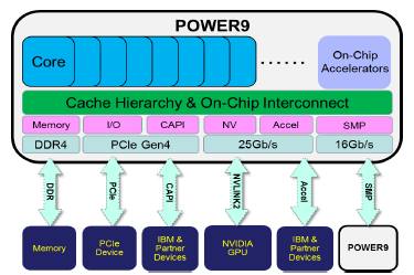
On the I/O front, the Power9 processors will also support PCI-Express 4.0 peripheral controllers, and that will mean a bandwidth bump for I/O in general and for the second-generation Coherent Accelerator Processor Interface (CAPI) overlay that IBM has to allow for shared memory between accelerators and the Power cores. IBM will also be opening up the accelerator bus that underpins the NVLink 2.0 interconnect, which will run at the same 25 Gb/sec speeds per lane in each direction, and creating a generic accelerator bus that other types of devices will be able to link to rather than go over the CAPI bus.
One thing that we are unclear of is how memory sharing with NVLink 2.0 and CAPI 2.0 will work with the Power9 main memory. Many different devices will be trying to share memory where it is rather than moving it between devices, and this could be very tricky indeed.
The performance specs for the Power9 SO chip look like it will be a staunch competitor to Intel’s future “Skylake” Xeon E5 v5 processor, due perhaps in the fall of next year. As we have previously reported, the top-bin Skylake part is expected to have 28 cores. As far as we know, Intel is only supporting PCI-Express 3.0 controllers on Skylake, but it is boosting the aggregate number of lanes from 40 to 48 to get extra bandwidth into the processing complex from the outside world. Intel does not have anything like CAPI or NVLink, but it could certainly come up with them. Intel is not as keen on selling accelerators as it is positioning Xeon and Xeon Phi processors with integrated networking for specific workloads; the company is also very keen on pushing hybrid Xeon-FPGA chips in those places where a hybrid Power-GPU setup might be able to show some good numbers.
This fight is far from over, and both Intel and the OpenPower collective have very different ways of looking at how systems will be designed in the future. The good news is that at least it is a fight, and IBM and its partners are doing some real engineering to give Intel some real competition – perhaps the first it has seen in many years in the datacenter, in fact.


VMware Widens Its Road To The Cloud With Google Partnership
Google and VMware have announced a new element to their partnership that the two companies said will simplify cloud migrations, provide more flexibility, and help companies modernize their enterprise applications with a minimum amount of pain. An expanded partnership between VMware and Google Cloud means AWS and Dell are being …

Power To The Kubernetes People
Big Blue shelled out an incredible $34 billion to buy open source infrastructure software juggernaut Red Hat, and it is determined not to just tend and grow that business, which brought in around $3.85 billion in sales in 2019 as the deal closed and probably somewhere around $4.6 billion in …
Can IBM Get Back Into HPC With Power10?
The “Cirrus” Power10 processor from IBM, which we codenamed for Big Blue because it refused to do it publicly and because we understand the value of a synonym here at The Next Platform, shipped last September in the “Denali” Power E1080 big iron NUMA machine. And today, the rest of …
I do not see IBM removing its on CPU vector processors, as that will be needed for those that do not have a need for Nvidia’s accelerators. I think that IBM is not as far enough along with HSA types of compute to the degree that AMD may be with its Server/workstation/HPC APUs on an interposer, where I think that at some point in time that AMD will engineer an APU on an interposer that can directly dispatch FP instructions to its GPU accelerator/s.
Having an APU on an Interposer presents a lot of potential to allow for a separately fabbed CPU/cores Die to be wired up more directly to the GPU, with the CPU cores complex and the GPU sharing a unified memory/Cache controller and the Zen cores Cache able to transmit entire cache lines to the GPU’s cache via thousands of parallel traces. We already see this with HBM and HBM’s thousands of wide parallel traces to the HBM stacks via the interposer, so say there where to be a direct CPU cache to GPU cache wide parallel direct connection with a unified cache controller complex on each respective CPU and GPU die working together to transfer instructions in need of FP work directly to the GPU and keep things completely coherent. It would not be hard to directly wire up these caches via the interposer’s silicon substrate as if the CPU and GPU where made on the same monolithic die.
I think that IBM will rely more on die process shrinks and maybe the Power8’s packed decimal arithmetic units may be the thing that could go to make way for other circuity on the power9’s, but that depends on just much of the legacy code base that remains that needs these units!
SIMD isn’t going away – and Power9-oriented commits to upstream compilers have indicated that VSX is actually getting a significant boost in Power9.
http://lists.llvm.org/pipermail/llvm-commits/Week-of-Mon-20160201/329664.html
Wow things must be going really great at IBM otherwise they wouldn’t cut their workforce by 18-25k. I think Power9 is as dead in the water before it even sees the light of day.
It’s not the IBM power9s that you like to make light of as being from only IBM that will be giving the lower cost competition, it’s the OpenPower licensed by third party Power8s/9s that will be competing ARM licensed IP business model style with Xeon SKUs! Also let’s wait for the server benchmarks before we Jump to the OranjeeGeneral-ization of things. IBM is not the sole supplier of Power8 or soon to be Power9 SKUs! IBM is now much like ARM Holdings the design bureau for all that is Power, but not all that there is for the supply of Power based server parts.
Do not underestimate the transformative power that the licensed IP business model will have over the entire CPU/GPU/other markets in the years to come. Like the ARM based market for mobile market players dwarfs Intel in total market cap and R&D spending the OpenPower based market will likewise do the same with the OpenPower base market players, Google/Others included!
HW is cyclical at IBM, and it has a very solid customer base. Now, they want a piece of the hyperscale market, and they are going to take it. Very interesting the open power initiativa.Lots innovation in just three years.
VMX or decimal is not going anywhere. Too much headache changing ISA compatibility. Also, just check the 3.0 document…
I’m very curious about this ‘execution slices’… what is that? throughput oriented design like GPUs? … looking forward to see what it is…
Geopolitcally The Power Chips microcode is open and this is something important to the national security of many nations. They don’t want to see back door code and this processor offers an open door to prevent such clandestine efforts.. Unlike the other guys Proc’s..