

If it was as easy as global replacing a bunch of MIPS cores with a bunch of ARM cores, then network chip makers Cavium and Broadcom would already have long since put their respective “ThunderX” and “Vulcan” 64-bit ARM server processors into the market. But creating a new platform is a bit more complex than that, and the ramp for both has taken longer than many expected.
But Cavium is now entering production for its first generation of ThunderX chips and is seeing design wins among motherboard and system makers, and early adoption in the HPC community, and so we thought it was time to do a profile of Cavium in our ongoing ARM Servers series. (We will get to Broadcom, Applied Micro, Qualcomm, Marvell, and the handful of others in due course, and have already covered AMD and did an opening essay on why we are still waiting for ARM servers.)
At the recent ARM TechCon in Santa Clara, we heard time and again that many of the top hyperscalers have substantial proofs of concept underway using ThunderX chips, but of course the big eight – Google, Amazon, Facebook, Microsoft, Baidu, Tencent, and Alibaba – do not talk about the hardware they have under test or the workloads they are putting through the paces. They have no doubt also tested Applied Micro’s X-Gene 1 and probably X-Gene 2, and may have also taken AMD’s “Seattle” ARM server chip out for a spin. It is reasonable to assume that the hyperscalers do not want Intel to know their plans, and they certainly don’t want their competition to know. But everybody suspects that the hyperscalers are deep into testing with ARM servers and Intel has been reacting as if they had them in production for several years now, so it comes to the same. At this point, the IT industry would be best served if the hyperscalers just came clean and showed their initial results, if they have any, and allowed us to see real world comparisons.
Thankfully, government sponsored HPC labs talk about what they are doing, so as ARM chips make their way into clusters for simulation and modeling, we will be able to see what is going on.
ARM Servers Plus Hyperscale Switching
Cavium was founded in 2001, just after the dot-com bust, as a fabless maker of semiconductor chips aimed mostly at the networking and service provider arena, where cheap compute needs to be embedded in myriad kinds of devices for shifting and shaping bits as they flit around the network. Cavium went public in 2007 with 125 employees, and today has over 900 employees and revenues of $413 million in the trailing twelve months. Cavium has posted losses as it has invested in expanding its product portfolio to include ARM products and because of stiff competition in the networking arena as Intel has been very aggressively moving into the space with its Atom and Xeon processors. The company pushed back in the black in the most recent quarter, with revenues of $105.1 million and net income of $4.2 million.
The company’s Octeon line of 64-bit multicore MIPS processors have been well received among network equipment makers, and indeed, it is the most recent Octeon chips that give Cavium the experience to build ARM based chips suitable for not just network devices, but also for serving and storage applications. We joked a bit about global replacing MIPS cores with ARM cores to turn an Octeon into a ThunderX processor, and it is not precisely untrue even if it is a vast oversimplification.
Back in February 2012, Cavium rolled out the Octeon III processor, which had up to 48 cores running at 2.5 GHz and delivering up to four times the throughput of the prior 32-core Octeon II generation of MIPS processors that it sold. Cavium created its own cnMIPS superscalar cores, based on licensed intellectual property from MIPS Technologies, the chip business that was spun out of supercomputer maker SGI that is now part of Imagination Technologies. The Octeon IIIs cram a lot of functionality onto a single die – a so-called system on chip – and had over 500 different kinds of function accelerators wrapped around the cores as well as controllers for networking and various kinds of I/O devices.
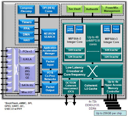
The Octeon III was no slouch on the memory front, with four DDR3 controllers and around 75 GB/sec of memory bandwidth across its 256 GB of capacity per socket. The Octeon III had another 500 Gb/sec of bandwidth available for PCI-Express, Ethernet, SATA, and other peripheral interfaces. Perhaps as significant as the memory and I/O bandwidth was the low latency coherency architecture that Cavium had developed, which could lash up to eight of these Octeon III processors together into a coherent NUMA system.
The Octeon IIIs were very interesting processors indeed, and like other chips such as the many-cored chips from Tilera, many of us were hopeful that they could jump the gap from the network aisle to the server aisle in the datacenter. This has not happened with the Octeons, and it was not something that Cavium was pushing for anyway, but it is happening with the ThunderXs and it is very much something that Cavium is aggressive about. Frankly, with AMD not providing an alternative to Intel’s Xeon, something has to fill the competitive pressure vacuum and it looks like it will be a slew of ARM chips and possibly a Power chip or two.
Our point is, if you squint your eyes looking at the ThunderX chip, you can see its Octeon III forbear. This is probably not a comparison Cavium likes to hear, but we would point out that Cavium’s success with the Octeon family is what is giving prototypers playing with ThunderX chips the confidence that the chip maker knows what it is doing and has the ability to sustain a chip business to deliver ARM server chips in volume and at competitive prices.
You won’t see the resemblance to the Octeon III immediately from the ThunderX block diagram, which is a bit skinny on the details:
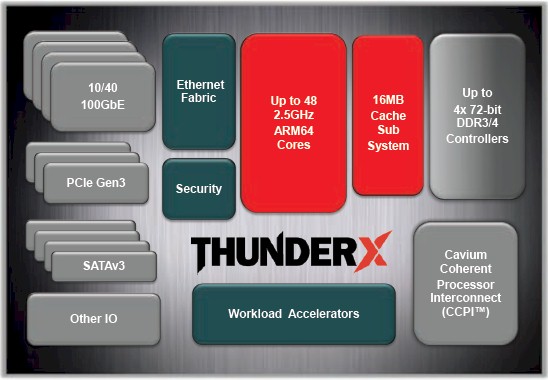
Even though the ThunderX chip was demoed in November 2014 at the SC14 supercomputing conference and started sampling in December to customers who were building reference platforms, and that the volume production of the ThunderXs is set to begin this month, Cavium is still being cagey about some of the precise feeds and speeds of the chip.
The ThunderX chips are being etched by Globalfoundries, the former AMD foundry operation, using a 28 nanometer process. Cavium is a full licensee of the ARMv8 architecture from ARM Holdings, much as it had a full license to the MIPS architecture. In both cases, this allowed Cavium to make significant changes and enhancements to the ARM and MIPS cores, so long as they did not break compatibility with the architectures. Cavium is using a custom ARM core, which has 78 KB of instruction cache and 32 KB of data cache per core and 16 MB of L2 cache that is shared across all of the cores on the die. The ThunderX will have from 24 to 48 cores, presumably delivered in increments of 6 or 12 depending on how chip yields go, but possibly at a finer granularity. The cores are designed to scale up to 2.5 GHz speeds.
The chip has four memory controllers, just like the Octeons, but supports both DDR3 and DDR4 memory instead of just DDR3. Each ThunderX chip can support up to 512 GB of memory per socket, which suggests that the chip supports two memory sticks per channel and a maximum capacity of 64 GB per stick. The DDR4 memory can run at a top speed of 2.4 GHz, the same as X86 servers. And like the X86 chips from Intel and AMD, the ThunderX chip includes circuits to perform virtualization tasks in hardware to isolate compute, memory and I/O resource isolation; this functionality is called virtSOC by Cavium. Cavium has said that the ThunderX will have hundreds of accelerators, just like the Octeons. We don’t know how many transistors are on the chip, or how many PCI-Express lanes, Ethernet ports, or SATA ports are implemented. But we suspect it will look a lot like the Octeons.
The Cavium Coherent Processor Interconnect (CCPI) for NUMA clustering on the ThunderX chips only scales to two sockets, but we suspect that it is very heavily based on the interconnect originally developed for the Octeons and can scale further if and when Cavium needs it to. With the bulk of the market using two-socket machines, it seems unlikely that this will be necessary out of the chute as the initial ThunderX chips ramp.
“Two socket is a major differentiator for us, and a significant number of our customers are interested in it,” Gopal Hegde, vice president and general manager of the Data Center Processor Group at Cavium, tells The Next Platform. “It puts us very close to the incumbent, high volume CPUs that are out there in the market, and it also allows a lot of our customers to reuse the platforms they have developed already. If they have a chassis and a power supply, all they have to do is redesign the motherboard. If you look at our ODM platforms, they are all in the standard motherboard form factors – MicroATX, EATX, ATX – that go into lots of different machines. And for the end users, it results in a machine that looks very much like what they are deploying today.”
As we have pointed out before, people do not want to change their processor architecture, their physical infrastructure and its management, and their systems software stack all at the same time. They might do two of them. So keeping the form factors and management the same is key for ARM chip adoption in the datacenter. (Ditto for Power chips, while we are thinking about it.)
The ecosystem for ARM servers is starting to come together, with software suppliers doing their ports and motherboard and system makers stepping up to create the iron. The development releases of Ubuntu, Fedora, and openSUSE Linux as well as FreeBSD Unix are available on the Thunder chips, and Ubuntu Server 14.04, SUSE Linux Enterprise Server, and a development release of Red Hat Enterprise Linux 7.2 are as well for those who prefer commercially supported operating systems. (There are persistent rumors that Microsoft has or will port Windows Server 2016 to ARM, but none of the ARM chip makers or Microsoft will comment on that. The KVM and Xen hypervisors work on ThunderX, and so does the OpenStack cloud controller and the OpenJDK and Java 8 runtimes for Java. Allinea and PathScale have moved over their application development tools.
On the hardware front, ODMs Gigabyte, WiWynn, Inventec, and Mitac have all created motherboards or systems based on Thunder, too, and Mellanox Technology has paired its InfiniBand and Ethernet adapters to the processors, Nvidia its Tesla GPU coprocessors, and SanDisk is flash storage.
And so, for Cavium, the ARM ramp begins.
“We are expecting to see revenues starting this quarter, and the ramp is going to be in 2016 and beyond,” says Hegde. “If you look at all of the open source software that we support, it covers a fairly significant part of the server market, maybe 20 percent to 25 percent. The cloud is growing, and there is a lot of interest in ARM in the high performance computing space with Cray, Lenovo, and Penguin Computing. A lot of things have to happen to reach 25 percent share, but I don’t see why not. None of us have a crystal ball. The way we look at it, we daily, weekly, monthly, quarterly, and annually build it, step by step.”
Hegde says that the ThunderX chip has over 40 customers (who can be server makers or hyperscalers) in development right now, and no one is naming names.
Network Effects
The Ethernet fabric that is implemented on the ThunderX chip is interesting, but don’t get the wrong idea. Cavium is not implementing an XPliant switch on the ThunderX chip, but rather the network ports that can reach out and talk to the XPliant-based switches (or other Ethernet switches) seamlessly.
The ThunderX chips will support Ethernet ports running at 10 Gb/sec, 40 Gb/sec, and 100 Gb/sec speeds. The 25G standard pushed by hyperscalers came out after Cavium divulged it was working on the ThunderX chips and presumably quite a bit of time after it had started working on its first ARM chips. So that probably explains that. The on-chip Ethernet fabric with the first generation of ThunderX chips can implement server node clustering with 2D or 3D torus topologies, says Hegde. Cavium is not detailing the aggregate bandwidth on the chip coming off these Ethernet ports, but we suspect that the chip will have 100 Gb/sec of aggregate Ethernet bandwidth, which can be cut up into 10 Gb/sec, 20 Gb/sec, and 40 Gb/sec segments as need be in the server design (25 Gb/sec and 50 Gb/sec segments may or may not be possible).
Perhaps the most important thing about the Cavium design is that is supports the same AMI MegaRack baseboard management controller that is used on X86 servers, and therefore, as much is possible in a Linux environment, a two-socket ThunderX machine has the look and feel of a very familiar X86 box to the hyperscalers, HPC centers, and enterprise customers who will be the early adopters.
And for now, very little benchmark data is available to allow direct comparisons between the ThunderX chips and their Atom and Xeon competition. When the Thunder project was announced in the summer of 2014, Hegde said that an eight-core ThunderX would consume about 20 watts and that a 48-core chip would consume about 95 watts, and that when you build systems out of Xeon and ThunderX chips, for a given unit of performance, the ThunderX platform would have around a 50 percent thermal advantage. We don’t know how well that comparison will hold up to the impending “Broadwell” Xeon E5 v4 chips due early next year or the “Skylake” Xeon E5 v5 chips due in 2017.
Cavium is not tipping its hand on what it knows about performance, either, except in a very general sense, until more customers put it through the paces. No one has run SPEC CPU tests formally on the ThunderX chips – we wish they would, just for fun. But this is serious, too, and Hegde explains why.
“The SPEC tests are CPU and memory benchmarks, and they are important because if you look at generations of server users, they look at these tests as a gatekeeper,” Hegde says. “But this is not a true measure of their performance, because a lot of the cloud workloads, for instance, are not just about CPU and memory. There are a lot of other things that go into making their workload run better. The benchmarks are typically CPU and memory bound, and a lot of them fit nicely in the cache, but if you go to the cloud, the dataset is so big the dataset cannot fit into the cache. In fact, the large cache increases the latency to memory and the hyperscalers sometimes turn it off. But still, if you go in with a very poor SPEC number, this is the measure they use as a gatekeeper, they will say no thanks, you won’t meet our performance requirements. If you are in the SPEC ballpark, then that discussion shifts to their workload.”
Speaking very generally, Hedge says that for traditional benchmarks like the SPECint integer test, a ThunderX chip is comparable to a Xeon E5-class processor, with performance points scaling down from there into the Xeon E3 range. When you look at cloud workloads – which are highly multithreaded, according to Hegde – and they also have a lot of network and storage I/O and using accelerators for OpenSSL and other functions. Add it all up, and for these vaguely defined cloud workloads, the ThunderX can beat a Xeon.
But again, we would all like to see the tests. (Back then the ThunderX chips were announced, the 48-core ThunderX was estimated by the Linley Group to have a SPECint2006 rating of about 350, and a 10-core “Ivy Bridge” Xeon E5-2470 v2 has a rating of about 375; a “Haswell” Xeon E5 v3 would do a little better than that.) And while we are thinking about it, we would love to see a full SKU list with feeds and pricing, just like Intel offers.
Cavium has four different flavors of ThunderX chips, and all four will offer up to the full 48 cores. (The original plan was to have one set of chips at 16 cores and another at 48 cores, but this has changed.) The ThunderX CP variants are aimed at web serving, content delivery, web caching, and data analytics workloads. The ThunderX ST variants are aimed at block, object, and Hadoop storage workloads, as well as distributed file systems and cold storage, and have special storage accelerators activated. The ThunderX SC are about “secure compute” and have various security accelerators enabled, while the ThunderX NT versions are aimed at media serving and network function virtualization workloads and support 100 Gb/sec ports. Hegde says that around 60 percent of the current customers playing around with the ThunderX chips are using the CP or SC versions aimed at compute, with about 20 percent testing the ST storage variant and the remaining 20 percent testing the NT networking version. None of these chips have brawny cores or heavy floating point capabilities, but that is the point. Cavium would suggest that companies offload to GPUs to get cheaper flops, and it is not trying to take away all the jobs that Xeons can do – and do well.
One last thing: Cavium has said very little publicly about its roadmap, but Hegde says that the ThunderX2 processor is under development, which will be implemented using an undisclosed FinFET (3D transistor) process from an undisclosed fab partner. (The only real options are Global Foundries, Samsung, and Taiwan Semiconductor Manufacturing Corp, which are all working on 14 nanometer processes with 3D transistors.) The ThunderX2 chips are expected to start sampling in 2016, and will no doubt mesh with the Xpliant hyperscale switching tightly. We also presume that the process shrink will allow Cavium to boost the cores and maybe the clock speeds, too.

Power Efficiency, Customization Will Drive Arm’s Role In AI
More than a decade ago, executives at Arm Ltd saw the energy costs in datacenters soaring and sensed an opportunity to extend the low-power architecture of its eponymous systems-on-a-chip that has dominated the mobile phone markets from the get-go and took over the embedded device market from PowerPC into enterprise …
Making Dollars And Sense Of Arm Holdings
The only thing stronger than having absolute control, as happens in monopolies and oligopolies, is the strength that comes from numbers. Both are economic principles as well as technical ones, and they both come together powerfully in the IT sector in general and in the semiconductor industry specifically. In this …
India Declares CPU Independence With Aum HPC Processor
At the moment, the most powerful Arm processor on the planet is the 48-core A64FX processor from Fujitsu, which was created as the heavily vectored compute engine for the “Fugaku” supercomputer at RIKEN Lab in Japan. Nvidia is getting ready to ship its 72-core “Grace” Arm CPU, which has yet …
FreeBSD supports Cavium ThunderX. FreeBSD on AARCH64! Woop Woop! That’s right, “Unix” on 48 Arm cores. Sweet…
https://community.arm.com/groups/processors/blog/2015/07/07/enabling-freebsd-on-aarch64
https://wiki.freebsd.org/arm64
AMD’s “Seattle” server chips are just transitional until the K12 cores arrive, so AMD will at least have the ARMv8A software stack ducks in order for its custom ARMv8A running micro-architecture K12 design, and hopefully a much wider order superscalar K12, those ARM 57’s can only decode/execute 3 instructions per clock. It’s interesting that some custom MIPS designs are getting SMT, and hopefully AMD’s K12 will have that SMT ability also, to get better CPU core execution resources utilization compared to the non SMT enabled custom ARM/MIPS designs that have yet to implement SMT.
I’m much more interested in what kinds of custom ARM K12 based server APUs will be available from AMD and paired with their new GCN Arctic Islands GPU micro-architecture on an interposer with HBM memory, and the ARMv8A ISA based K12 cores wired up more directly to its GPU accelerator via some wide parallel traces on the interposer’s silicon substrate. If the HBM on an interposer can see 4, 1024 bit wide parallel traces from currently the GPU to HBM with relatively low memory clocks 500MHz (1000MHz effective falling and rising clock edge of the 500Mhz clock) for 4 HBM stacks at a total memory bandwidth of 512GB/sec, then what about the CPU cores wired up to the GPU with an even wider than 4096 direct parallel traces and whole blocks of data/code transferred directly between CPU and GPU via the interposer etched traces.
So via an interposer/interposer technology if a CPU can be more directly wired up to a GPU, how long will it be before a CPU can directly send/dispatch a FP instruction(pre-encoded into the GPUs ISA), or Int instruction directly to the GPUs FP/INT units to be worked on, processed, and directly sent back to the CPU for further processing of some final results on the CPU.
It will be possible with a wide parallel direct BUS between CPU and GPU for the CPU to send whole blocks of data/code to the GPU’s parallel ranks and files of FP/INT/other execution units to be worked on without having to transverse any extra PCI/other data protocol encoding/decoding steps using a more direct pathway and saving much latency and power required for those uncore types of transfers normally done via PCI/other protocols.
So AMD’s custom K12 CPU server cores may/may not be equivalent or better than Cavium’s/others’ custom ARM server cores, but what about the advantages that having a server chip/GPU accelerator on an interposer package and the ability to more directly connect up the CPU cores to the GPU FP/INT/other units in a more direct way than over the PCI/other protocols that are currently in use for GPU acceleration workloads. I’d imagine that a CPU ARM, x86, or other, with a more direct pathway to and from the GPU could even forgo storing the work/GPU kernels to RAM, and could directly dispatch/receive whole blocks of data/code to and from the GPU directly(into/from the GPU’s cache), and putting any accelerated workloads done via PCI/other to shame.
So with an interposer a totally separate CPU, and GPU die can be wired up like a current APU is with its CPU and GPU on a single monolithic die. Imagine for some future APU’s on a single die being even more HSA compliant with the CPU/GPU so integrated with each other that the CPU’s FP/other units are actually the GPU’s FP/other units, with the CPU functionality so completely merged with the GPU functionality, that the CPU part of the APU can and does dispatch FP/INT/other work directly to the only FP/INT/other units available on the shared units on a fully merged CPU/GPU.
On a much more powerful and flexible basis take this level of CPU/GPU, and even FPGA/other, integration to the Interposer and have separately fabbed CPU core blocks wired up to separately fabbed GPU/other blocks with the interposer providing the silicon substrate to wire things up that same more direct logical monolithic die way and that is going to eventually put the old way of GPU compute acceleration over PCI/other protocols at a serious disadvantage.
AMD does not have any claim/rights to doing things on an Interposer, but AMD appears to be the one getting the interposer based SOC/APU to a market introduction in advance of others having to do the very same thing, for servers and PCs, and probably laptops and other mobile devices.
It’s to early to tell and it will probably be 2020 before a real ARM based server leader can even be hinted at with so much new custom ARMv8A ISA based IP coming on the market, and that Interposer technology will become very important by 2020 and beyond.
So, everything in AMD has been transitional(not only Seattle). Perhaps they can transition to the bankruptcy filing soon.
Judging by the lack of real world products using AMD’s Seattle (outside of development systems) and the lack of mention for AMD’s K12 in the last earnings conference call and recently at the Raymond James technology investors conference, IMHO that K12 is probably scrapped and was never completed at all. Taking also into account the amount of time Jim Keller had at AMD, with only 3 years, just not enough to work on multiple projects including Seattle, (cancelled) Skybridge, Zen and K12. After completion of AMD’s Seattle, most likely AMD is only concentrating on Zen only all that time which is why project Skybridge was cancelled and I suspect K12 was cancelled as well…
This statement seems very unlikely to be true:
“Speaking very generally, Hedge says that for traditional benchmarks like the SPECint integer test, a ThunderX chip is comparable to a Xeon E5-class processor, with performance points scaling down from there into the Xeon E3 range. ”
When comparing a 2-wide in-order core against an out-of-order much wider Xeon E5 with an aggressive memory hierarchy.
I suspect Cavium are bending the truth by comparing SPECintRATE benchmarks. By bait and switch to that kind of throughput benchmark, where the latency of any given thread isn’t reported, they can look good on a per-socket or per-machine basis.
But, the exact essence of the “brawny versus wimpy core” debate, which Urs Hoezle settled, was that latency in scale-out matters too much in the cloud for the wimpy cores to win.. no matter how many you have!
I don’t know what clock speed hyperscale Xeon cores run at, but if they’re limited to ensure they stay inside the power budget, perhaps the Cavium ARM cores have a MHz-per-Watt advantage that might offset any inherent disadvantage vs. Xeon?
The 2699 V3 and 8890 V3 run at 2.8GHz+, so there’s not really a disadvantage for Intel on clocks
Example of “brawny cores versus wimpy cores” here http://www.anandtech.com/show/9185/intel-xeon-d-review-performance-per-watt-server-soc-champion/13 look at the response time, especially Intel’s “brawny” Xeons versus Intel’s “wimpy” Atom C2750. Unfortunately the test was not performed on Applied Micro’s X-Gene but already can guesstimate how it will perform (which is similar to Intel’s Atom C2750). As for power consumption, example here http://www.anandtech.com/show/9185/intel-xeon-d-review-performance-per-watt-server-soc-champion/16 with Intel’s 14nm and 22nm FinFET advantages, those ARM chips using 28nm or 40nm process nodes are not going to be able to compete here. The lack of benchmarks and performance-per-watt from Cavium themselves to showcase their ThunderX is already quite telling. That is why Cavium is talking about using GPGPUs and accelerators…