

The “Knights Landing” Xeon Phi processor from Intel will be shipping by the end of the year and ramping in volume through 2016, and it is set to shake up the systems market in a number of significant ways.
The chip will be the first commercial processor with very high bandwidth memory right next to the CPU, and it will also cram dozens and dozens of cores onto a die, making it suitable for all kinds of parallel workloads that are constrained on memory bandwidth. A variant of the chip will also have an integrated 100 Gb/sec Omni-Path interconnects, giving it very high I/O bandwidth.
Here at The Next Platform, we think that the Knights Landing processor will find lots of uses outside of the very high end of the supercomputing market, given all of these and other features. In fact, we think that the Knights Landing chip is the vanguard of a wave of processor and packaging designs that will eventually be introduced to the market. A mix of near and far main memory with various bandwidth plus stages of non-volatile 3D XPoint and NAND flash memory looks like the memory hierarchy of choice for a server node for the next couple of years. This is what happens when you take a mono-socket microserver form factor and give it an appropriately useful amount of compute, memory, and I/O to do real work. And if the software stack moves far enough to the left, we could be seeing the use of two-socket servers decline for a lot of workloads. (Intel’s own vast EDA chip design farm is moving from two-socket back to one-socket machines for performance and software licensing reasons, but EDA likes fast single-threaded performance so Knights Landing may not be the right choice.)
While Intel is always cautious about positioning its processors against one another, and it does not like to show preferences, what is clear is that the Xeon Phi engineers and architects expect a broad audience for Knights Landing. It will come down to packaging, pricing, and the availability of systems and application software tuned to ride its cores and eat its memory and I/O bandwidth.
We don’t know how Knights Landing will be priced – a key aspect of the processor and co-processor that will gate its success – but we are learning more about the features in the Knights Landing chip and its packaging. Intel gave The Next Platform a relatively deep dive on Knights Landing back in March, showing off the chip package and the architecture of the die and its memory architecture. We have since then pondered the ramifications of the near and far memory on the Knights Landing package, and talked about the momentum that is building for this chip, which is a true processor as well as being an optional co-processor.
At the Hot Chips 27 conference in Silicon Valley this week, Avinash Sodani, chief architect of the Knights Landing chip at Intel, gave some more insights into the impending parallel processor and also privately revealed some other goodies about the chip.
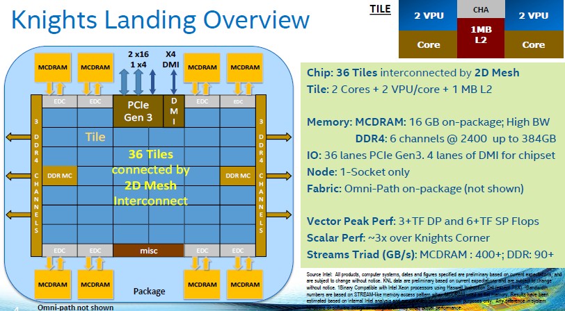
As many of us had suspected from the get-go, the rumors that the Knights Landing chip would have as many as 72 active cores on a die turned out to be true, which Intel confirmed during the ISC 2015 supercomputing conference back in July. Here’s the fun bit: Sodani told The Next Platform after his presentation that the Knights Landing Xeon Phi processor actually physically has 38 dual-core tiles on its die, for a total of 76 cores. The Knights Landing chip is at the beginning of the 14 nanometer process ramp at Intel – along with the “Broadwell-D” Xeon D server chip aimed at microservers for hyperscalers – and that means the yields are not as high as they can be. So Intel put in some extra cores, Sodani explained, so if there are chunks of logic that do not work it can heal around them and still deliver a maximum of 72 active cores for its top-end Knights Landing parts.
There is nothing at all unusual about this. Precisely the same thing happens in the Xeon processor line at Intel and IBM does likewise with its Power8 chips; ditto for Nvidia and AMD GPU chips. Prior generations of Xeon Phis had 61 cores, but Intel sold variants with 57 or 60 cores activated at speeds of 1.05 GHz, 1.1 GHz, and 1.24 GHz. We expect that a more broad range of Xeon Phi chips will come to market with the Knights Landing generation, with different near and far memory configurations, core counts, clock speeds, raw floating point performance, and form factors. As we have discussed before, there are three different types of Knights Landing chips coming to market, with two being able to boot up as a standalone processor and the third being aimed at coprocessors that are similar to the Xeon Phi 3100, 5100, and 7100 series based on the “Knights Corner” predecessor to Knights Landing.
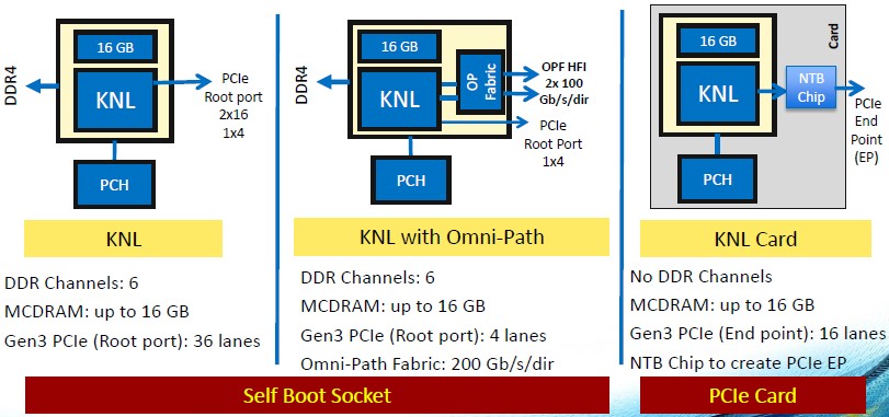
As you can see, the base bootable Knights Landing chip has 16 GB of MCDRAM high bandwidth memory right on the package and DDR4 memory controllers to link out to a maximum of 384 GB of regular DRAM memory. The chip has two PCI-Express 3.0 x16 ports and one x4 root port as well as a southbridge chipset to link to various I/O devices. The Omni-Path interconnect is not on the chip itself, but is rather implemented in the package, with each PCI-Express x16 port having its own bi-directional, 100 Gb/sec ports. Each port can deliver 25 GB/sec of bandwidth in both directions. Integrating an InfiniBand or Omni-Path interconnect directly on a Xeon or Xeon Phi die (or any processor) is a bit tricky, so Intel is integrating on the package first as a means of lowering the overall cost and power consumption in the Knights Landing platform. (Oracle is, however, etching two InfiniBand ports into its future Sparc T “Sonoma” chips for scale out clusters, so it can be done.)
The free-standing Knights Landing co-processor card will put a non-transparent bridge (NTB) chip on the card, linking to the processor through one PCI-Express x16 port, as a PCI-Express endpoint. This version of the chip will also have its DDR4 memory channels deactivated and will only have the 16 GB of MCDRAM near memory for the processor to access. It is unclear if all of the memory modes developed for Knights Landing will be supported in the coprocessor, but given the latencies of moving data over the PCI-Express bus, we suspect not. If the price on the free-standing Knights Landing cards is small enough, it is possible that these sell well, but we expect most enterprises, hyperscalers, and HPC centers will be interested in the self-booting versions of the Knights Landing chips, not the coprocessors.
One of the things that Intel has not yet divulged is a good set of block diagrams of the Knights Landing internals, but Sodani showed a bunch of them off at Hot Chips this week:
As we explained back in March, the Knights Landing core is based on a “Silvermont” Atom core that has been so heavily modified that Sodani says it probably should have its own code name. This chip support four-way simultaneous multithreading, twice as deep as the HyperThreading used in the Xeon family of server chips.
Intel is not being precise, but says that the modified Silvermont core will deliver around three times the single-threaded performance of the Knights Corner core; this is important because real Windows and Linux operating systems and the single-threaded portions of applications have to be able to boot on these cores and run with acceptable performance. “Many times, one thread per core is enough to reach peak performance,” said Sodani, so the threading is dynamic and will change as workloads demand. This modified Silvermont core will have ISA compatibility with the Xeon family and can run any application on a modern Xeon without recompilation.
Across all 72 cores, the Knights Landing chip will deliver more than 6 teraflops of single precision and more than 3 teraflops of single precision performance thanks to the two AVX512 vector processing units that are welded onto each core. (They can process 32 single precision and 16 double precision operations per clock per core.) The Knights Landing chip is the first of Intel’s Xeon family that will have support for this AVX512 vector processing unit, but we expect it to be added to the future “Skylake” Xeon E5 v5 processors.
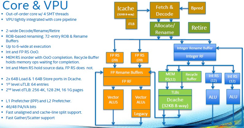
Intel has not said what the relative size of the Silvermont cores and AVX512 units are, but we suspect that these vector units will be pretty big. What Sodani did say is that the vector units were tightly integrated with the cores, not hanging off to the side, and this was one of the reasons why the Knights Landing core cane execute up to six instructions per cycle even though it has a two-wide pipeline.
The Knights Landing cores have a Cache/Home Agent that sits on the 2D mesh interconnect on the Knights Landing die that keeps the 1 MB L2 caches on all of the tiles coherent. This mesh is something we expect Intel to possibly use as the basis of massively parallel processors in the exascale era, as Intel Fellow Shekhar Borkar discussed hypothetically at ISC 2015 a month ago. As Intel’s current Xeon chips demonstrate, the on-chip ring architecture is getting more and more complex as cores and caches are added to the dies; at some point, a mesh will probably make more sense. (Not for a few generations, perhaps.)
The Knights Landing mesh, we learned at Hot Chips, will operate in three modes: all-to-all, quadrant, and sub-NUMA. In all-to-all mode, addresses are uniformly hashed across all distributed cache directories. This is the most general mode with the easiest programming model, but it will offer lower performance than the other modes. In quadrant mode, the Knights Landing chip is divided into quarters and addresses are hashed to directories in the same quadrant; the operating system has no idea this is going on underneath the covers, and it provides lower latency and higher bandwidth for the cores running in each quadrant. In sub-NUMA mode, the operating system exposes all four quadrants as virtual NUMA clusters, which makes a Knights Landing chip look sort of like a four-socket Xeon server. This mode provides the lowest latency, but applications have to be NUMA-aware and care has to be taken with memory pinning to get the maximum performance.
As we pointed out above, the Knights Landing chip will run a superset of instructions that are compatible with Xeon chips. Here is how they overlap:
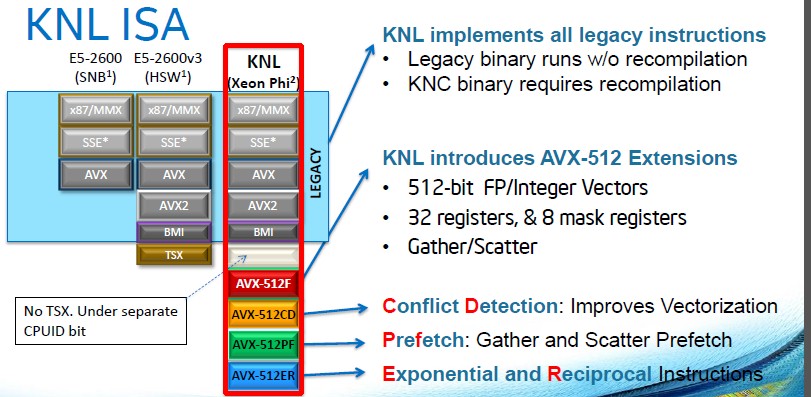
The transactional memory (TSX) features that have been added to some of the “Haswell” Xeons are not supported with the Knights Landing cores. But, as Sodani revealed, there are a slew of new 512-bit vector instructions, which will no doubt be added to future Xeon processors, too, in good time. One set of instructions provides hardware assistance for the scatter/gather functions that dominate simulation and modeling workloads that are based on the Message Passing Interface (MPI) protocol. Here are the details Intel provided on the other vector functions that will debut with Knights Landing:

While raw floating point and integer performance is an important aspect of the Knights Landing design, memory bandwidth is perhaps the driving force behind the architecture. Intel has not provided the raw bandwidth of the MCDRAM or DRAM memory blocks, but has said it can get more than 400 GB/sec of bandwidth out of the 16 GB of MCDRAM and more than 90 GB/sec out of the regular DRAM attached to the chip running the STREAM Triad memory bandwidth benchmark.
How does this compare to Knights Corner? The top-end, 61-core Xeon Phi 7120X has a peak memory bandwidth of 352 GB/sec out of its 16 GB GDDR5 memory, and on STREAM tests run by Intel, this co-processor was able to deliver 177 GB/sec of memory bandwidth. By the way, a two-socket “Ivy Bridge” Xeon E5 server topped out at 87 GB/sec on the STREAM Triad test, and a two-socket “Haswell” Xeon E5 machine could push it up to 110 GB/sec. So the DRAM far memory on the Knights Landing chip is in the same ballpark as the Xeon E5 in terms of sustained memory bandwidth and the near memory is more than twice that of Knights Corner Xeon Phi coprocessors. Applications will get the best of both worlds – and without having to buy two Xeon processors.
To whet the appetite for Knights Landing processors, Sodani divulged some early benchmark test results that pit the 72-core Knights Landing chip against a two-socket server using the 14-core Xeon E5-2697 v3 processors, which clock at 2.6 GHz. (Intel has not disclosed the clock speed for the Knights Landing chip, but we think it will vary from 1 GHz to maybe 1.3 GHz.) So that is 72 cores on a die with something on the order of five times the memory bandwidth of a machine with 24 cores. Here is what the performance looks like:
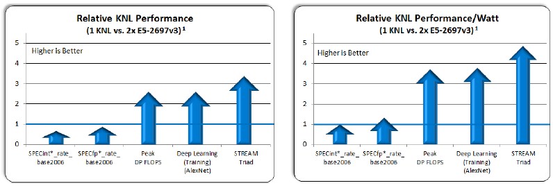
In this chart, Sodani confirmed, the relative performance figures that Intel has are at the tip of the arrow – you have to be precise in this world – and Sodani adds that the arrows indicate they can go up. (We suspect they will by Knights Landing launch day, which we expect perhaps at the SC15 supercomputing conference in Austin in November.) As you can see, on raw integer and floating point SPEC tests, the Knights Landing chip is a little bit behind those two Xeons, but for peak double precision and deep learning workloads, it is about 2.5X the two Xeons and on the STREAM test it is getting close to 3.5X. The Knights Landing chip is expected to have a thermal rating of 200 watts, and the two Xeons are 145 watts each, and if you adjust this performance by the wattage consumed, then the Knights Landing chip is at parity more or less on the raw SPEC tests and is far superior for floating point, deep learning, and STREAM tests.
The question now is: What will Intel charge for a Knights Landing chip? It has to be low enough to compel customers to buy it and port their code, but it can’t be so low as to undercut its Xeon business. Or, Intel can be aggressive, charge a lot less than a GPU costs, and let the Xeon and Xeon Phi chips lay where they may.

Intel Hedges Its AI Bets With Habana Labs Buy
Intel has made another big move toward its ambition to dominate the artificial intelligence space in the datacenter, acquiring Israeli AI chipmaker Habana Labs for $2 billion. The amount dwarfs the $350 million or more Intel paid for AI chipmaker Nervana Systems back in 2016. Which leads us to the …

Aurora Rising: A Massive Machine For HPC And AI
As long as great science gets done on the final incarnation of the “Aurora” supercomputer at Argonne National Laboratory, based on Intel’s CPUs and GPUs but not on its now defunct Omni-Path interconnect, people will eventually forget all of – well, most of – the grief that it took to …
Can Nvidia Be The Biggest Chip Maker In The Datacenter?
Next year, with the launch of the “Grace” Arm server processors, Nvidia will have all of the compute and networking bases it cares about in the datacenter covered, and it will be selling its technology at a rapid pace. Nvidia already has a larger datacenter business than AMD has – …
due-core tiles -> duo-core
delete comment
KNL integer performance shown above (as measured by SPECint_rate_base2006) doesn’t look good at all – it seems to be the same or even lower than of a pair of Xeon E5-2650 v3 (10 cores / 20 threads / 105W / $1,050 each).
And while high network performance of KNL is good in general, 2x100Gbs per KNL CPU may be an overkill except for some HPC workloads.
And unfortunately, there’s no self-boot version with 2x50Gbs networking and 20 PCIe x3 lanes
Which will still set it miles above any nVidia or AMD GPU out there. I think the question comes down to will you buy a Xeon + GPU or just a XeonPhi. I would bet the latter gives you the better choice overall.
The 2.5x double precision FP advantage over dual socket Xeon will only last until Skylake EP. At that point you get AVX-512, doubling FP, and additional cores and IPC improvements over Haswell EP will likely bring it to parity. Then it comes down to relative system costs, and the potential benefit of the high speed memory for the specific workloads being considered.
Unless Knights Hill has AVX-1024! HA! Then we have Knights always having more floating point, provided the core counts work out.
But seriously.
I agree about the memory. Knights will be for workloads that can be networked relatively loosely and that need high bandwidth memory on a single compute socket, and perhaps one in the future that only has high bandwidth memory (generic term, not a brand) and then maybe gobs of 3DXP and NAND off to the side. The other end of the spectrum will be Xeon machines with lots of cores, maybe an FPGA, a mix of standard DRAM and 3XDP behind that, on the same memory controllers perhaps, adding capacity and non-volatility while also offering bit addressibility.