
The announcement this week by Intel and Micron Technology of 3D XPoint memory, which will sit somewhere between DRAM and NAND flash in future systems, has everyone thinking about the architectural, economic, and performance implications of emerging memory technologies in devices of all kinds – including those humming away in the datacenters of the world.
This is obviously something that CTOs all over the world think about, but Dean Klein, who has that job at Micron, probably has more insight than most on how current and future memory technologies will be stacked up to create a new memory hierarchy in systems. The hierarchy is getting taller and more complex, which presents as many issues as it seems to solve.
Klein was on hand at the ISC 2015 supercomputing conference in Frankfurt, Germany recently to talk about the issues and how myriad emerging memory technologies might be deployed. He did not mention 3D XPoint specifically, which Intel and Micron have been collaborating on since 2012, but he did talk generally about the “tweener” emerging memory that he believes will slide in between DRAM – or possibly hierarchies of DRAM – and NAND flash devices.
“We are putting so much investment into emerging memories, collectively as an industry, that something is going to emerge,” Klein declared, and the fact that Intel and Micron were showing off 3D XPoint wafers and committing to delivering samples of this tweener memory later this year is just one example. “Something will come out of this. Economically, these are tweener technologies, at least initially. I think this is an opportunity. How we integrate these into the system, how programmers can take advantage of the characteristics of the memory they are addressing is an opportunity that exists for HPC and for other systems.”
The big issue, and one that all creators of innovative memory technologies have been wrestling with, is not only are these new memories technically challenging, but they also pose formidable economic challenges. There has to be sufficient volume to justify the investment, and the manufacturing process and the use conditions have to be similar enough to existing DRAM and NAND that they can be made by fabs and used in systems similar to those available today.
The State of DRAM and NAND Flash
To get a feel for those challenges, Klein reviewed the state of the DRAM and NAND industries, where Micron participates. There are a lot of forces at play that compel the choices that system and storage vendors make.
“There is limited new wafer capacity in the system today,” Klein explained. “There are not a lot of new fabs being built. What we are seeing is demand for diversified, differentiated memory systems, and that is driving demand in a little bit different directions than it has in the past.”
The PC industry has been the traditional driver of the DRAM market in the past 35 years or so, and with the release of a new operating system and sometimes a new more powerful processor, the consumption of memory would go up and memory makers would build fabs to meet the demand. As Klein pointed out, over this long history, sometimes the capacity outstripped demand, and sometimes governments supported the research into memory making equipment and the building of fabs. The resulting oversupply conditions were jarring to the industry.
“We would be shipping memory at a loss and making it up in volume,” Klein quipped. “Today we have favorable memory market conditions, where the supply and demand are approximately balanced. But PC demand is not there, however. It has virtually cratered, but what we are seeing is these new platforms – smartphones, tablets, and so on – are certainly picking up the slack and have been the drivers for differentiated memory technology.”
We would point out that DDR4 memory was the first time we can recall when the server industry actually lead the charge with a new DRAM technology rather than fall in behind the PC industry after that technology matured. And we expect that emerging memory technologies will also be deployed in datacenters first and then find their way into other machines as they mature. The volume economics, to a certain extent, will be reversed, and that means the benefits will have to be proportional to the premium that datacenter customers will pay – and be willing to pay – based on those benefits.
Another factor affecting the DRAM market, which is also the case with the disk drive and processor industries, is the massive consolidation of suppliers over the decades. We could have economists arguing until the end of time about how this helps or hurts the commercial or consumer customers, but the fact remains that consolidation happens because technology progress gets more and more expensive and only the large can survive. Without such consolidation, Moore’s Law advances in technology and economics (it was always process and money) very likely would not be possible.
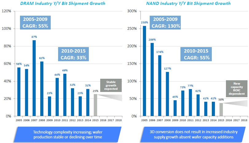
The complexity of the manufacturing process, says Klein, is driving the memory industry down to more stable and lower growth on aggregate bits shipped per year for DRAM.
The big issue with DRAM memory is that the capacitors that sit over a memory cell to store data have had to get taller and taller as chip processes have shrunk in order to maintain the same surface area of the capacitor and therefore maintain its capacitance. With an aspect ratio of 30:1 to as much as 70:1, these capacitors are shaped like inverted goblets, as Klein called them, with an access transistor at the bottom.
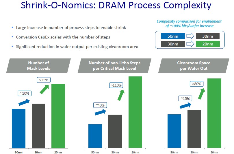
“That doesn’t come for free, and you can’t do that with a single mask step and it adds to the number of mask levels and the number of non-Litho steps per critical mask level, and it has the effect of reducing the number of wafers you can get out of a square foot of fab real estate. And fabs don’t come cheap – it is a $4 billion to $6 billion problem to build a fab.”
And NAND has its own issues too, says Klein.
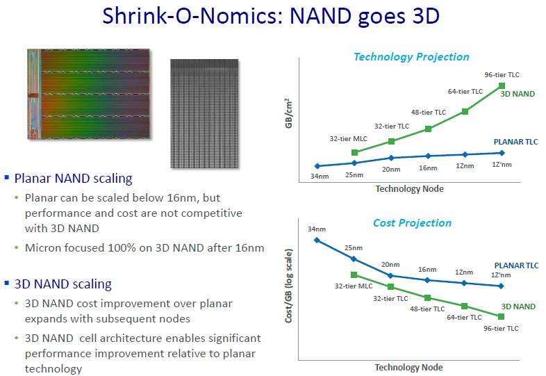
“NAND is going 3D, and this is definitely going to increase the number of bits we get on a wafer, but this, too, does not come for free. 3D NAND is similarly requiring more process steps to add those additional vertical parts on the device. We have a cost advantage coming with 3D NAND, and we ultimately get a density advantage, but we don’t get a bits out increase with 3D NAND.” There are other benefits to 3D NAND, too. The cell-to-cell interference goes way down with a 3D structure – the cells are further apart and they don’t interfere with each other as much. So error detection and correction gets easier.
The complexity of the chip etching process as we do the Moore’s Law shrink each generation is making the whole design and manufacturing process more expensive and time consuming. The double patterning techniques employed today use very complex mask structures, but it has enabled the chip industry to make features far smaller than the 193 nanometer wavelength of light used to etch masks – in essence, you use the masks to distort the light in precise ways that end up with much smaller features being put onto silicon wafers than you might otherwise think is possible. (We think of it as squinting through eyelashes and using the edge of an eyelash to correct for astigmatism, if you have had to do that as we have had to.) And this will not get better, but get worse with the extreme ultraviolet (EUV) techniques that IBM, GlobalFoundries, and Samsung have just tested at 7 nanometers and that Intel is also expected to use at 7 nanometers in some form.
“The reality is, extreme UV is not small enough to do away with this multiple patterning, either,” says Klein. “So if we implement extreme UV and then also accept the extremely slow throughput that it offers, which translates into a lot of money to expose these wafers, we would still have to do multiple patterning. So that is not a solution for us, either – and if it is, it is an expensive solution.”
Small wonder, then, that memory and storage makers are looking to new memory technologies and an expanded memory hierarchy to help create systems with better performance, thermals, and economics.
The Emerging Memory Contestants
Klein is a bit like a kid in the candy store talking about various memory technologies that are emerging to augment DRAM and NAND in systems. There’s conductive bridging RAM, ferroelectric RAM, phase change memory (PCM), polymer resistive RAM, polymer ferroelectric RAM, spin-transfer torque magnetic RAM, magnetoresistive RAM, metal oxide resistive RAM, carbon nanotube, and molecular memory.
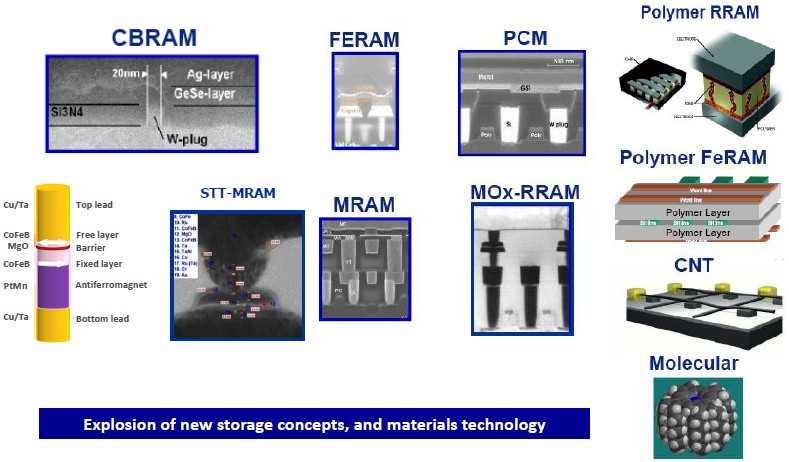
“There are a lot of possible candidates for emerging memory, but all of these are really interesting if you dig down into the mechanics of them,” said Klein. “With a PCM cell, imagine that we are melting glass at 600 degrees Celsius inside one of these cells, and yet it is scalable and on a chip level it is relatively power efficient. That’s amazing that we can do that sort of thing. But these other cells are no less interesting. The STT-MRAM is very interesting in that we have built a magnet next to a piece of magnetic material that we can flip, and by running current through this we can flip these magnets around. It is a fascinating technology.”
All of these emerging memory technologies – just like the 3D XPoint memory Intel has just announced – share common characteristics and common challenges in being brought to market. Let’s rattle them off.
They are all more expensive than NAND flash – every one of them – and Klein cautions to not think of them as replacements for NAND. They all offer more endurance than NAND, and STT-MRAM offers very high, DRAM-like endurance, according to Klein. Most of these emerging memory technologies are in that in-between space where they have more endurance than NAND – a measure of how frequently you can overwrite the memory cells –but do not have as much endurance as DRAM.
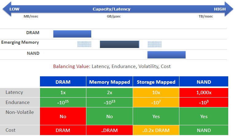
All of these new memories are slower than DRAM, and they have greater activation energy than DRAM as they flip bits. They all offer – with STT-MRAM being the possible exception – less endurance than DRAM. But they are all less expensive than DRAM, too, even if they are all more expensive than NAND flash.
As for non-volatility, which means being able to power it down and still have it retain data and which is a key requirement for many uses of these emerging memories, Klein said they generally can be used as non-volatile memory but that he preferred to look at these as semi-non-volatile because many of these are not stable for the length of time that we expect NAND to be stable. All of these new memory technologies need some sort of error correction, whether it is done at a word level or a block level, which will depend on the application. They all offer potential byte or word addressability – unlike NAND, which is only block addressable, and unlike DRAM, which is bit addressable.
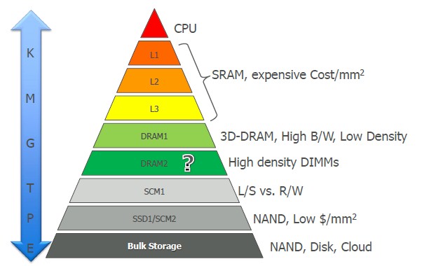
So where will these new memory technologies fit into the hierarchy of storage in systems? Right about where you would expect, given their performance and cost. “My belief is that they fit in between SSDs and DRAM, and DRAM may have a hierarchy unto itself,” says Klein, adding that he foresees fast stacked DRAM, perhaps, on processor chips and near DRAM and far DRAM further out, then stretching out to storage-class memories. The important thing will be to have the hardware and the operating system in the systems manage the flow of data up and down that hierarchy.
“Where we put these in the architecture is going to determine how we use them, with either read/write semantics or load/store semantics,” explained Klein. There are plenty of architectural choices system designers are going to have to make. Will these be used for their non-volatility or not? Do they want memory-like performance or storage-like performance? Do they want to access this new memory with read/write or load/store methods? Will they have word or block error correction? Is it going to be cache-like or explicitly managed?
System architects have a lot to think about, and not just because of theory, but because Intel and Micron just put a stake in the ground with 3D XPoint and they are determined to bring it to market – whatever technology it is based on.

The Cheapest Compute In The Intel Xeon Lineup
While the minimalist server processor — and the microserver concept that was based upon it — did not take over the datacenters of the world, there are still some workloads that can fit in modestly powered single-socket CPUs just fine. That is why Intel has always created server variants of …
Industry Behemoths Back Intel’s Universal Chiplet Interconnect
When the hyperscalers, the major datacenter compute engine suppliers, and the three remaining foundries with advanced node manufacturing capabilities launch a standard together on Day One, this is an unusual, significant, and pleasant surprise. And this is precisely what has happened with Universal Chiplet Interconnect Express. The PCI-Express interconnect standard …
Intel Back To Playing The Long Game, Not The Wrong Game
The supply chain is holding back the server business, and not just in the way you are thinking. Yes, there is a limited supply of manufacturing and packaging capacity for server-class processors based on the most advanced semiconductor nodes. It’s in the less obvious ways, such as the availability of …
Be the first to comment