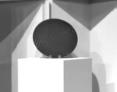
It is not an insignificant thing to announce an entirely new class of memory. After all, in the almost 60 years that memory has been manufactured, there have only been seven types that have emerged—all of which had different attributes that were improved upon in successive generations.
Today, during an announcement call with Intel and Micron on the new 3D XPoint memory, the expectation seemed to be that there would be so much doubt about the feasibility and manufacturability of something that is not DRAM, not NAND, yet offers a claimed 1,000x performance benefit over both with an equal improvement in endurance that they had to bring proof. Specifically, as Mark Durcan, CEO of Micron, and Rob Crooke, VP and GM of the non-volatile memory technologies at Intel, said, they wanted to show that this new memory class was not just a PowerPoint concept. It is in fact in the fab at the Lehi, Utah site where the two companies work on joint projects.
While the process might be different, the goal of the new memory variant from Intel and Micron is to bring as much data as close to the compute as possible. Durcan points to a few applications where this capability can be game-changing, including in areas as diverse as high performance computing simulations (enabling higher resolution, faster calculations), genomics (where the data volumes for comparative matching is critical), other large scale pattern recognition and machine learning algorithms, and even in gaming, where the drive for more fidelity and seamless gameplay is bottlenecked by the time it takes between memory and the CPU.
“This is not just a little faster, it’s a lot faster—it is also 10x or more the density of conventional memory and it is non-volatile so it can also be used as storage. The aim is to scale with computing; when we scale the CPU, the memory and data need to scale with it.”
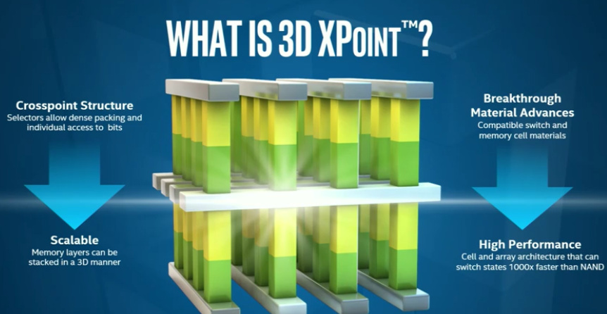
As the name implies, 3D XPoint memory is a unique cell architecture that is a crosspoint memory that can be stacked. Below is an example of a small section (at higher scale) of the first product in 2016 that will be 128 gigabit stacked in two dimensions, so two layers high. There will be 128 billion memory cells on each chip, which is not much different than high-volume NAND technologies capacity-wise and which works out to 16 GB. The uniqueness here is on the materials front and the new switch and memory cell design that lets Intel and Micron eliminate the transistors.
It’s easier to think of a crosspoint memory architecture like a screen (as in doors or windows). Where two wires cross, imagine a tiny pillar at each junction made of a special material that consists of a switch and memory cell. This architecture can then select each memory cell individually, which means read and writes can happen at the individual pieces of memory levels. That can all happen quickly, and it is interconnected by metal lines that allow for fast access and activation, which creates a much different and higher performance architecture. This is where the note about the materials sciences breakthrough is important. Although we are not aware about what the materials are at each layer of the “screen” in this case, nor the connection pillars, chances are they offer key advantages in terms of conductivity.
Although the presentation was light on the nuts and bolts details about what enables the kind of speed and endurance characteristics in 3D XPoint memory, when it emerges for public view sometime in 2016, chances are we will get a better sense in the context of some real world applications. It is even possible that some of what was announced today is a key to what we will see on the future CORAL supercomputers (when they describe innovative memory approaches that they could not detail a few months ago). What Intel and Micron did say is that the key to these performance and endurance breakthroughs is the result of new materials innovations. Crooke jokes that in simulating and testing the new materials for the 3D XPoint memory they could have used the technology to aid in far more detailed views of how the materials would perform.
One question might be how this is entirely new architecture-wise outside of the materials angle. Further, how might this compare to the 3D NAND flash that was announced earlier in the year? Durcan says that the announcement of the 3D NAND flash was more of a modification of existing NAND technologies but this is different in that it allows news ways of computing, tiering of memory, and entirely new applications. Since it can be used as both main memory and storage and has a much higher density and number of writes that are possible, he says it opens the door for applications that they have not even begun to dream up yet. “It’s writable in small amounts, so it can act like memory as well as storage, but it’s like NAND in that it is non-volatile. This means it can be used as wicked-fast storage but with far greater performance and endurance.”
Durcan points to the number of application areas from genomics to HPC to gaming that suffer from the same type of memory bottleneck. He says that what is entirely new here is that once that bottleneck is reduced, once the systems can be balanced between CPU, memory, and memory bandwidth, the efficiency and performance improvements will lead to far more capable applications, whether those are scientific simulations or massive online multiplayer games.“Other memory technologies would do two of three things really well,” Durcan explained. “They were non-volatile and very dense, or they were dense and fast. But what we need, and what we have developed, is something that is all three—it’s dense, fast, and non-volatile.”
The interesting bit will be to talk to system architects about where 3D XPoint memory will fit into the memory hierarchy, and what effect it could potentially have on application performance. So we will be trying to find out more details about 3D XPoint memory and talking to system builders to see what they think this new memory will do for machines.


According to the press release Intel denies this is a memristor – so it will be very interesting to see what new ground this represents, or whether this is a marketing effort. It is clear from similar efforts at HP and others using memristor technology that this offers similar gains. Odd that the initial product is only two layers. if they can produce 32 layers of NAND, the having only 2 layers here suggests a constraint on managing voltages across the array at depth. Hope this is not another LCOS.
The HP Machine architecture was never dependent on memristors – it’s pride was. This technology will presumably slide right in, provided it has enough of the same write properties as it was expecting from memristors. And when and if memristors go commercial, HP can change again. The idea is to have a single pool of addressable memory that is persistent and linked by silicon photonics to compute.
Hmm sounds like this could be the end of HP’s memresistor and their “The Machine” architecture if this really ships next year HP is in serious trouble as it ticks all the boxes memresitor ticks as well. But I don’t think HP will roll out anything before 2017 at best.
Yes, it felt strange that HP anounced delay with The Machine almost at the same time they anounced Intel partnership. I wonder what the details of that partnership were …
Was this the new memory that Intel was talking about with the Purley platform for upcoming Xeons?
I’d imagine that this will replace flash burst buffers, or at least add another tier to them.
I’d also imagine that HP could build something more like the original memristor based Machine instead of the DRAM only revision if they can integrate this before it launches(or just delay The Machine).
However, if Purley and Knights Hill deploy this before The Machine, then it kind of makes The Machine a lot less revolutionary.