
Update: 5:08 p.m. Eastern – We have been able to dig into more details about the system architecture and confirm Knights Hill architecture and other interconnect/system details. Update detail page can be found here.
For the first time in over twenty years of supercomputing history, a chipmaker, as opposed to a systems vendor, has been awarded the contract to build a leading-edge national computing resource. This machine, expected to reach a peak performance of 180 petaflops, will provide massive compute power to Argonne National Laboratory, which will receive the HPC gear in 2018.
Supercomputer maker Cray, which itself has had a remarkable couple of years contract-wise in government and commercial spheres, will be the integrator and manufacturer of the “Aurora” super for Argonne. This machine will be a next-generation variant of its “Shasta” supercomputer line, which it has been designing in conjunction with Intel since the chip maker bought the Cray interconnect business three years ago for $140 million.
The new $200 million supercomputer is set to be installed at Argonne’s Leadership Computing Facility in 2018, rounding out a trio of systems aimed at bolstering nuclear security initiatives as well as pushing the performance of key technical computing applications valued by the Department of Energy and other agencies.
This is the third and final announcement for pre-exascale class systems under the CORAL initiative, a $525 million undertaking that was announced in 2014 to bring a new generation of large-scale systems into play that will set the stage for future machines, which the DoE expects to be capable of pushing exaflops somewhere in the 2020 to 2022 timeframe. CORAL is a collaboration involving three national labs in the United States–Argonne, Oak Ridge, and Lawrence Livermore–with inter-agency support from the Department of Energy, the National Nuclear Administration (NNSA), and the Office of Science.
The machine at Oak Ridge National Laboratory, called Summit, will be delivered in 2017. It will provide over 5X the performance of the current top system at the lab, the Opteron and GPU-powered Cray XK7 Titan machine (also the second most powerful supercomputer on the planet) in one-fifth the number of nodes. The new Summit machine is expected to push 150 to 300 peak theoretical petaflops—a significant improvement over Titan, which tops out at 27 petaflops. The CORAL supercomputer at Lawrence Livermore National Laboratory, named Sierra, which is also set to be installed in 2017, will provide over 100 petaflops of peak performance.
For context, the relative performance of existing DoE supercomputers is below. Recall as well that the current top machine at Argonne is the Mira supercomputer, which delivers 10 petaflops peak while drawing 4.8 megawatts of power. Its successor, Aurora, with its 180 petaflops peak will pull 13 megawatts. This is an 18X performance improvement in performance with just 2.7x the power. During interviews today we will hopefully be able to extract how many nodes and cores this Aurora machine will have.
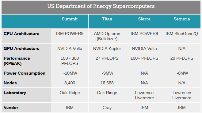
Both of these other CORAL machines sport a similar architecture that is based on IBM Power9 chips, which will emerge just in time with delivery of these systems. The performance and efficiency boost will come from Nvidia Volta Tesla GPUs with Mellanox EDR InfiniBand hooking the hybrid Power-Tesla nodes together. Two key features of the Volta GPU are stacked memory and NVLink interconnect, both of which are important for keeping the processors on both the Power and Tesla components fed.
All of this begs the question, if IBM, Nvidia, and Mellanox have collaborated to provide performance on these two earlier systems, it only stands to reason that with a delivery year of 2018, the Aurora machine will sport a different architecture (generally for multi-system procurements there is a mix of system design and vendors for balance). By the time 2018 rolls around, there is one architecture that appears to be most fitting, although it has only been a glimmer in Intel’s eye as it continues development of the predecessor architectures, Knights Landing and Knights Corner.
Knights Hill is the third in this generation of processors that so far have only found a real home in large-scale supercomputers, even though Intel is predicting and engineering the Knights processors for an expansion into enterprise markets. Further, Knights Hill will very likely mark a significant performance improvement over the Knights Landing processors that will be found in two other upcoming DoE supercomputers, the Trinity and Cori machines.
Intel has not said much about the future Knights Hill massively parallel processor, and very likely will not until it is about a year away from shipping the part in systems, if history is any guide. But to get the supercomputing labs and other possible commercial customers to start investing in the Knights chips, Intel had to provide some kind of roadmap that extended out beyond the impending Knights Landing chips, which it did last fall at the SC14 supercomputing conference. We have learned a lot more about Knights Landing in the past month, and that gives us some clues as to what can and will be done to create Knights Hill, which is very likely the motor inside of Aurora.
Just to review, Knights Landing has at least 60 heavily modified “Silvermont” Atom cores, which have a pair of 512-bit AVX2 vector math units attached to them. The rumor is that Knights Landing will have 72 cores, which means 144 of these vector units. Yields and thermal envelopes being what they are, it seems likely that Intel will not ship Knights Landing parts with all 72 cores activated; we expect clock speeds in the range of 1.2 GHz to 1.3 GHz if the core count is relatively low and slower if the core count is higher. The main thing is that Intel wants to have the Knights Landing chip hit more than 3 teraflops, which is triple that of the current “Knights Corner” coprocessor. The Knights Landing chip will have 16 GB of high bandwidth memory hooked to the same 2D mesh that links all of the cores together, and also has two DDR4 memory controllers on the mesh that link out to up to 384 GB of memory. (This near and far memory can be addressed in a number of ways, as we explained last month.) The important thing is not just local memory, but high memory bandwidth. Avinash Sodani, chief architect of the Knights Landing chip at Intel, told The Next Platform that the DDR4 far memory has about 90 GB/sec of bandwidth, which is on par with a Xeon server chip, and that 16 GB of HBM delivers more than 400 GB/sec of aggregate memory bandwidth.
The 2D mesh on the Knights Landing chip is new for Intel, and when asked about how far it could scale, Sodani said that the architecture could scale for two to four generations for sure. And when we suggested that Intel could, in theory, create NUMA-capable Xeon Phi processors but that it made far more sense to just add more components – cores, memory controllers, and HBM ports – to this 2D mesh and ride down the Moore’s Law curve, Sodani did not say we were wrong and moreover, said that making NUMA machines would not be possible because the bandwidth of memory requests across the NUMA interconnect would utterly swamp the processor interconnect. So, that tells us Knights Hill will have more cores, and as many cores as the process used to etch it will allow.
Intel has said that Knights Hill will use a 10 nanometer process, which is the one it will be ramping later this year for its processors for various client devices. The shift from the 14 nanometer processes used with Knights Landing to the 10 nanometer processes used with Knights Hill probably won’t yield a big change in core counts or clock speeds – maybe something on the order of a 30 percent to 50 percent boost in cores (call it somewhere between 90 and 100 cores) and about the same clock speed (somewhere around 1.2 GHz). Intel could keep adding more AVX vector units to the custom Silvermont cores to boost floating point performance, but has said that it wants to show pretty decent integer performance with the Knights chips, too. So it seems unlikely it will let them get too far out of balance after just getting them into balance with Knights Landing.
That’s another way of saying that Knights Hill might deliver somewhere between 4 teraflops and 4.5 teraflops of peak floating point performance. It is safe to say that local memory on the package and addressable through DDR controllers – as well as bandwidth on these memories – will scale proportionately.
Intel has also said that Knights Hill will support the second generation of its Omni-Path networking, which very likely runs at 200 Gb/sec if it is to compete against the HDR InfiniBand switching from Mellanox Technologies, due in the late 2017/early 2018 timeframe.
As noted previously, we are set to talk to Intel and Argonne for more details. Both conversations are happening as you read this. Updates and confirmation on these and other architectural speculations made here will be coming soon.

The Era Of Big Memory Is Upon Us
If you reduce systems down to their bare essentials, everything exists in those systems to manipulate data in memory, and like human beings, all that really exists for any of us is what is in memory. We can augment that memory with external storage that preserves state over time, but …
With HPC Humming Along, HPE Awaits Its AI Boom
The ProLiant server business is down in the dumps, and the storage business is in a slump. But petascale and exascale supercomputer deals based the combination of AMD CPUs and GPUs have filled in a lot of the gap. And Hewlett Packard Enterprise is now waiting, like all OEMs and …
Intel Decides To Engineer Its Fab-Filled Future After All
Newly anointed Intel chief executive officer Pat Gelsinger held the coming out party for his strategy to get the world’s largest chip manufacturer and designer back on track, called “Intel Unleashed: Engineering The Future,” on Tuesday after the market closed. It was a strange echo of an essay we wrote …
Hi. This one went to a chipmaker because only chipmakers were allowed to bid in the Coral procurements as primes. The prior two Coral opportunities (ORNL, LLNL) went to IBM, who were able to bid as a chipmaker (Power).
That is a good point–I should have clarified at the beginning that this is the first time a chipmaker that isn’t also a systems vendor has scored a contract like this in a couple of decades.