
The first of the server processors based on Intel’s “Broadwell” cores and using its 14 nanometer chip making processes comes to market today. The launch of the Xeon D chips gives IT shops a new option in building dense machines for hyperscale workloads. This also offers a glimpse into the cores that will be used in future Xeon E5 and E7 processors aimed at a wider array of workloads.
The Xeon D chip, developed under the code-name “Broadwell-DE,” is also the first Xeon chip to leverage the component convergence ideas of system on chip, or SoC, designs, which have been popularized by makers of MIPS, ARM, and PowerPC chips used in embedded and networking devices. A half dozen 64-bit ARM chip suppliers that have expertise in networking want to get into the more profitable server space in a big way. The idea is to take the fight to the ARM market at the moment that the ARM collective is bringing the fight to Intel.
The Broadwell cores are a tweak to the Haswell cores, which made their debut in the Xeon E3-1200 v3 processors for single-socket servers back in January 2014 and in the Xeon E5-2600 v3 processors that came out last September. Haswell is a new core implemented in the tried-and-tested 22 nanometer processes, and Broadwell is a derivative that is implemented in a smaller 14 nanometer process. On desktops, the process shrink and design changes resulted in around a 30 percent improvement in performance per watt, and having that energy efficiency come through with a performance boost at the same time is something that hyperscale datacenter operators want to see for sure, and probably more than a few supercomputing centers and enterprises, too. We will have to wait for the Broadwell-EP and Broadwell-EX a while longer – Intel has not even shipped a Haswell-EX in the Xeon E7 family yet – but it is good to get some insight into the architecture before these more mainstream chips come along.
Instructions Per Clock Advance Again
No matter the chip architecture, clock speeds are capped because of thermal limits imposed by the heat density of the chips and the difficulty of removing that heat. Energy consumption and therefore the heat dissipated by chips rises exponentially with clock speed, and that has caused all chip makers to add cores as they shrink transistors rather than cranking up clock speeds. This means applications either have to get more parallel or more applications have to be added to a single machine with management software to get them to share the capacity efficiently. Having said that, chip designers are also trying to get more work done per clock.
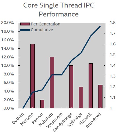
Chris Gianos, the chip engineer who drove the development of the Haswell Xeon E5-2600 v3 and the Broadwell Xeon D-1500 for the past several years, put together this handy chart that shows how the number of instructions per clock (IPC) has gone up in the past decade for the cores that have been used in client and server processors from Intel, starting with the “Dothan” Pentium M cores back in 2004. Gianos said in a briefing with The Next Platform that the instruction set changes and microarchitecture tweaks in the Broadwell cores delivered about a 5.5 percent boost in IPC compared to the Haswell cores used in the Xeon E5s last year and in the Xeon E7s expected sometime this year.
As you can see in this chart to the right, the chips with a major architectural change in the cores, called a “tock” in the Intel parlance and always implemented in a chip making process that has been perfected on prior generations of client and server chips, show the biggest IPC gains. The “ticks,” as Intel calls the variants of the chip that involve a manufacturing process shrink and some tweaks to the architecture to boost performance, show lower IPC gains. The “Penryn” cores didn’t do hardly anything and “Westmere” got precisely zip over its predecessor, the “Nehalem” core. We can presumably expect a bigger jump with the “Skylake” cores that come after Broadwell. What you can see is that over a decade long period, Intel has been able to get just under two times as much work done per clock, and that is a feat.
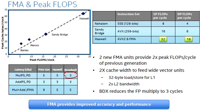
The Haswell cores had support for 256-bit floating point and integer math in the AVX 2.0 units, and had dual fixed multiply add (FMA) unit that provided twice as much performance in floating point math calculations compared to the “Sandy Bridge” and “Ivy Bridge” cores that preceded them. For those using floating point, there are some goodies in the new Broadwell core:
With the Broadwell core, Intel has cut back the effort it takes to do a floating point multiply operation to three clock cycles. (In the chart above, BDX is supposed to be BDW, which is the shorthand Intel uses for Broadwell.) The Haswell and Broadwell cores could handle 32 single precision or 16 double precision floating point operations per cycle. The top-end Xeon D-1540, which has eight cores running at 2 GHz, will deliver 256 gigaflops of raw double precision number crunching power – and do so in a 45 watt thermal design point. (We will get into how this might be interesting to some HPC customers in a separate story.)
The Broadwell cores also add in support for Intel’s Transactional Synchronization Extensions (TSX), which originally debuted with the Haswell cores but which was deactivated in the Xeon E5 v3 processors because of a bug. (TSX will be available in the upcoming “Haswell-EX” Xeon E7 processors, according to Gianos.) With transactional memory, Intel removes the locking mechanisms that keep threads from manipulating the same data in main memory and lets them complete their work. In a normal system, when data is used by a thread, it is locked so no other thread can touch it, and that means other threads can stall even if they are only reading the data. By eliminating the locks at the front end and doing checks only after threads are done with their work, applications can run a lot faster. For instance, on HPC workloads, TSX has been shown to deliver about a 40 percent boost in performance on clusters, and Intel has also done performance tests on SAP’s HANA in-memory database using TSX.
Intel made a lot of tweaks in the Broadwell cores that are going to be appealing to the gamut of server users, whether they can use the new Xeon D series today or have to wait for the Broadwell variants of the Xeon E5 and E7 chips in the future.
On the virtualization front, The Xeon D chips have a new feature called Cache Allocation Technology, which allows for the L3 cache on the chip to be partitioned so threads in one application that are behaving in a greedy fashion can’t mess with the cache memory segments used by other threads. (A chip is a lot like a server and as more cores and cache and coprocessors are added to the chip, Intel has to think of ways of virtualizing and managing the resources on a die, much like a hypervisor does with the resources in a server.)
Another Broadwell feature that is making its debut with the Xeon Ds is called Memory Bandwidth Monitoring, and it provides bandwidth-aware scheduling for jobs running on multiple cores in the Xeon D chip such that a mix of high-bandwidth and low-bandwidth jobs can be spread around the cores to keep memory bottlenecks from forming on one or more cores on the die. This feature can be used by operating systems and hypervisors, and in conjunction with virtual machines using the cache allocation feature mentioned above today and with main memory controllers on the Xeon processors in the future. Intel has also chopped the VM exit/enter latency of a hypervisor running on the Broadwell core to around 400 cycles, down from 500 cycles with Haswell cores, and has added a bunch of features to reduce the number of VM exits and interrupts in the first place. These exits and interrupts are a big part of the overhead of server virtualization.
Intel made a lot of tweaks in the Broadwell cores that are going to be appealing to the gamut of server users, whether they can use the new Xeon D series today or have to wait for the Broadwell variants of the Xeon E5 and E7 chips in the future.
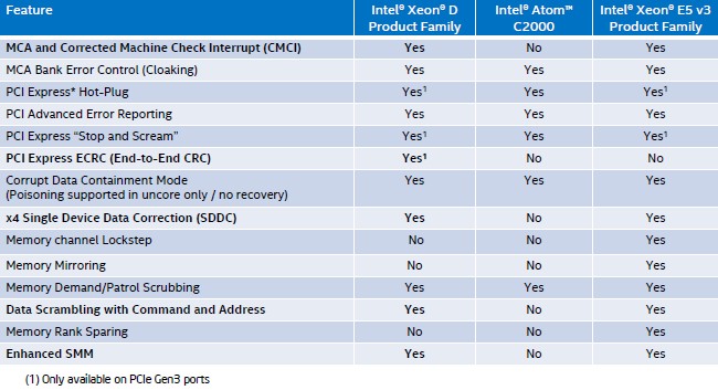
The Broadwell cores have a random seed generator, which is a better way to create a lot of random numbers for simulations than was possible with prior Xeon cores, and also has new crypto instructions that boost the performance of RSA public key encryption and decryption by around 30 percent. A new feature called Intel Processor Trace captures information about software execution and branching in the CPU as it runs to help debug applications. Intel has also improved error correction for DDR4 memory and PCI-Express I/O, and has a new hardware controlled power management feature on the Broadwell cores that allows an operating system to guide power management better than the firmware controlled P-state performance controls and C-state CPU controls of the prior Xeon chips. Those P-states, which scale the voltage and frequency up and down, and C-states, which put various parts of the chip in stasis, still work. But the new hardware power states allows an operating system to make much quicker decisions and do it without having to resort to an authority outside of the server to figure out what power state to put the machine in.
There are a slew of features that boost the reliability, availability, and serviceability of the Xeon D-1500s, and here are how those stack up compared to the existing “Avoton” Atom C2000 and Haswell Xeon E5 v3 processors:
That explains what the new Broadwell Xeon cores look like, now we can step back and see what components are integrated in the Xeon D processors. In a separate story, The Next Platform will examine the markets that Intel is going after with the Xeon D chips. We will also take a look at how these SoCs might be used outside of the corral that Intel has put them in.
Intel is making a Xeon-based SoC for one simple reason: It wants to offer a Xeon-based processor aimed at microservers as well as network and storage needs that is absolutely and completely compatible with other Xeon processors in its product line. While the server variants of the Atom processors have many of the same features as other server chips, there are differences between the Atom and Xeon cores and these differences can be issues for companies looking to make or deploy microservers or networking or storage equipment. As Gianos puts it, the Xeon D SoC has “100 percent, real Broadwell cores,” and is therefore absolutely compatible with any and all software that is tuned to other Broadwell chips and is backwards compatible with earlier Xeons.
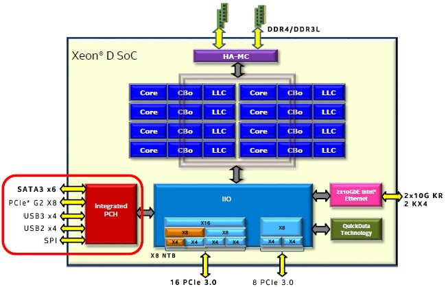
To call the Xeon D a true SoC is perhaps a bit of a stretch, since the Xeon D actually has two physical chips in its package. (Perhaps it is more accurate to call it a SoP, or system on package.) With the Xeon D, as you can see in the block diagram below, the memory controllers, cores, L3 caches, dual Ethernet, and various PCI Express 3.0 controllers are all on one die. Another chipset, part of what would normally be called a southbridge, for implementing legacy PCI-Express 2.0 peripheral slots as well as USB and SATA ports, is on a separate chip that is integrated with the Xeon D CPU complex through a dedicated link, perhaps similar to that which Intel used in the past to hook external but on-package GPUs to CPUs for laptops and desktops. The elements of that CPU complex are lashed together by a pair of high-speed rings, as all Xeons are these days. The rings are more extensible than a crossbar, which is why Intel does it that way.
By contrast, the Avoton Atom C2000 chip that is replaced by the Xeon D to a certain extent brought all of the components of the system, including the southbridge chipset for linking various external I/O peripherals to the processor and memory complexes, onto the die. This is what made it an SoC. That Avoton chip had eight of Intel’s “Silvermont” Atom cores (the same Atom cores ones that will be modified and used in the future “Knights Landing” massively parallel Xeon Phi processor and coprocessor), which were dropped in pairs with 1 MB of L2 cache each onto the die. The core and cache pairs were hooked to each other by a crossbar switch and linked to peripheral slots, including an embedded Ethernet controller running at 1 Gb/sec, through multiple layers of fabrics that ran at different speeds. It was an elegant but perhaps complex design.
The Xeon D, like other CPUs that bear that moniker, has three levels of cache memory instead of the two used with the “Centerton” Atom S1200 and Avoton Atom C2000 processors that came before it at the low-end of the server chip lineup from intel. It is this third level of cache that helps deliver the higher performance levels on a wide variety of applications compared to the Avoton Atoms. To be precise, the Xeon D has 32 KB of L1 data cache and 32 KB of L1 instruction cache per core, and then another 256 KB of L2 cache per core. There is an eight-way sliced L3 cache that weighs in at 12 MB for all of the cores to share, which is chopped up into 1.5 MB segments.
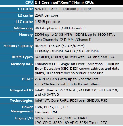 Like other Xeons, the two memory controllers on the die support 46-bit physical addressing and 48-bit virtual addressing, which means that the processors could in theory be linked to up to 64 TB of physical main memory if someone built a shared memory system using the Xeon Ds. (With no QuickPath Interconnect, or QPI, ports, which are used to do NUMA clustering on other Xeons, this seems unlikely.) The memory controllers support low-power DDR3 memory (1.35 volt) running at 1.33 GHz and 1.6 GHz and regular DDR4 memory (1.2 volt) running at 1.6 GHz, 1.87 GHz, and 2.13 GHz. Each memory controller has a single channel and can support two memory sticks on each channel. With 32 GB memory sticks in the RDIMM form factor, a single-socket node can support up to 128 GB across the four slots. With 16 GB sticks in the UDIMM or SODIMM form factor (which is used for very dense packaging) memory tops out at 64 GB across the four slots. Either way, for many workloads in the enterprise, hyperscale, and HPC datacenters of the world, 64 GB and 128 GB capacities are normal, if a bit on the skinny side for server buyers looking a few years out.
The Xeon D chip’s integrated PCI-Express 3.0 controller has six controllers with a total of 24 lanes of I/O, and these can be packaged up in a number of ways, as you can see from the block diagram above – anywhere from one x16 slot and one x8 slot for the highest bandwidth per slot to six x4 slots for the maximum number of slots, with several mixed variants in between. The off-die but on-package chipset has eight controllers with eight lanes of I/O. There are six lanes of 12 Gb/sec SATA 3.0 coming off this chipset.
Perhaps the most significant change between the Avoton and Broadwell-DE chips, aside from the shift in core type, is that the latter has two 10 Gb/sec Ethernet controllers etched on the die. These controllers are derived from Intel’s external Ethernet network interface cards, and implement a dual-port controller that can run at 1 Gb/sec, 2.5 Gb/sec, and 10 Gb/sec speeds and, importantly, uses the same Windows and Linux drivers as the external cards support. The integrated Ethernet controllers support Single Root-I/O Virtualization (SR-IOV) and Virtual Machine Device Queues (VMDq), two important I/O virtualization techniques that are employed by hypervisors these days. The network interfaces also support the VXLAN and NVGRE network overlay protocols, which allow for Layer 2 networks to be virtualized and stretched across Layer 3 networks, thus allowing for virtual machines to be live migrated across the larger network using the VXLAN and NVGRE tunneling methods. And finally, the integrated Ethernet supports the 802.3az energy efficient Ethernet standard for reducing power consumption when the network is not running full tilt boogie.
The Xeon D processors support Intel’s implementation of simultaneous multithreading, called HyperThreading or HT for short, which turns one physical instruction pipeline in the Broadwell core into two virtual ones to boost performance. All the other Xeon features, such as VT virtualization extensions and Turbo Boost overclocking, are also supported – again, this is a real Broadwell core, so this stands to reason.
Adding It All Up For A Big Performance Boost
At the moment, there are only two variants of the Xeon D processor available, but in the fall, Intel expects to roll out more Xeon D chips with features aimed specifically at networking, storage, and Internet of Things workloads. These three other members of the Xeon D family will presumably have different price points than those offered by the two server variants of the SoC, and again we presume they will be lower, too, because Intel is trying to expand the X86 architecture into these other markets.
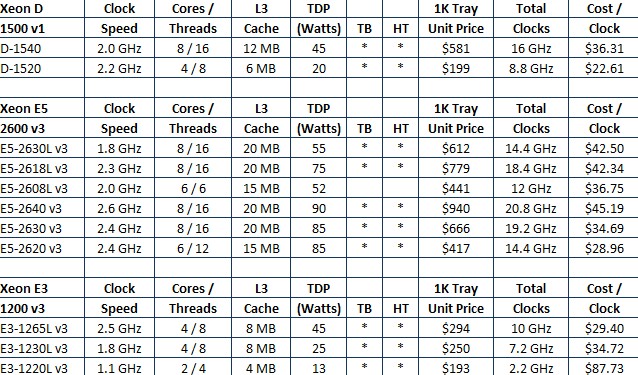
The Xeon D-1520 has four cores and a clock frequency of 2.2 GHz, with a Turbo Boost capability up to 2.5 GHz across all four cores and to 2.6 GHz with only one core boosting. Intel did not yet divulge the L3 cache on this chip, but it probably only has 6 MB of L3 cache; we know it has a thermal design point of 20 watts and costs $199 when bought in 1,000-unit quantities from Intel. The Xeon D-1540 has eight cores running at 2 GHz with the same Turbo Boost caps on the cores, has the full-on 12 MB of L3 cache, and it has a thermal design point of 45 watts. It has a price of $581 per 1,000-unit tray. Here is how the Xeon D chips stack up against the current Xeon E3 chips for single-socket machines and Xeon E5 chips for two-socket machines, which are both based on Haswell cores:
The aggregate CPU clocks shown above are just to give a very rough sense of the relative performance of the processors show. Obviously, all clocks are not created equal across Xeon chip generations or even within them, but this is a very rough reckoning of how the bang for the buck works out in a generic sense (not including the effects of HyperThreading). The Xeon D chips offer more performance and about the same power bands as the low-voltage variants of the four-core Xeon E3 chips. Intel is charging about the same, on a per-unit of performance basis, for the top-end Xeon D-1540 as it charges for a Xeon E5-2608L v3, which has six cores, no HyperThreading, and a slightly larger L3 cache but also a slightly higher wattage.
Intel used a pre-production variant of the eight-core Xeon D-1540 running at 1.9 GHz in its benchmark tests to see how this chip stacked up against the eight-core Atom C2750, which clocks at 2.4 GHz. Depending on the workload, the Xeon D-1540 delivers anywhere from a low of 34 percent more performance than the Atom C2750 to a high of 3.4X and at the upper end of that performance improvement, that works out to a factor of 1.7 better performance per watt.
On general purpose workloads, it looks like customers can expect a pretty significant performance bump from the Xeon D compared to the Avoton. On the STREAM benchmark that tests memory bandwidth, the Xeon D bests the Avoton by 78 percent and on integer throughput, as gauged by the SPECint_rate_base2006 test, the pre-production Xeon D does 2.63 times the work as the Avoton. With the Memcached caching program, expect a 127 percent bump, with static web serving increasing by 169 percent, according to Intel’s tests. Server side Java will run 3.15X faster, thanks in large part to the beefier cores and L3 cache memory, and dynamic web serving (like PHP workloads) will run 3.4X as fast and, significantly, offer around 1.7 times the energy efficiency per unit of work. This will be important for the hyperscale web work that Intel expects the Xeon D to run.
On the storage front, early tests comparing the top Avoton and Xeon D parts show a 34 percent increase in performance for large streaming I/O work on a server configured with 24 disk drives and a factor of 2.52 increase on work with small transactional I/O work. For networking, the Xeon D with four cores running at 2.2 GHz has about twice the L3 packet forward processing oomph with large packets and about three times with smaller packets running atop Intel’s Data Plane Development Kit (DPDK) for networking.
In general, based on the SPEC integer benchmarks, Intel says that the Xeon D chips will overlap between the high-end of the Xeon E3 line and the low-end of the Xeon E5 line. The most powerful Xeon E5, the E5-2699 v3, will offer 5.1X times the integer performance as the Xeon D-1540, just to give a sense of scale.
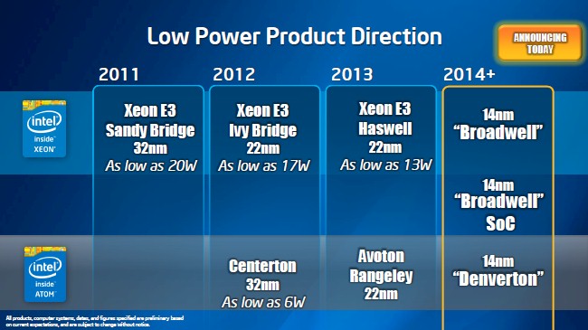
What Intel has not yet explained is how it will differentiate plain vanilla Broadwell-based Xeon E3 chips, which will not use SoC design concepts, and the future “Denverton” Atom C series chips, which will, from the Xeon Ds. All three of these chips will be based on 14 nanometer processes and will presumably be chasing many of the same customers and perhaps even used in similar systems.



You have “tick” and “tock” crossed over. I know what you said seems to make sense, but you must remember that Intel is a manufacturing company, and so the process change is more important than the micro-architecture. Therefore the “tick” is when the process changes, and the “tock” is when it doesn’t (but you have a new micro-architecture).
My dyslexia shows through. The clock goes “tick tock” and I do indeed think of microarchitecture first and process second, because one has to come before the other. Now I know to put a reversal on it. HA!
Good reporting overall !
However, I noticed some inaccuracies (if I am not mistaken):
– “had dual fixed multiply add (FMA) unit”: FMA stands for Fused Multiply Add
– “six lanes of 12 Gb/sec SATA 3.0”: SATA is still capped at 6 Gb/s per lane
Regards
Minor quibble: The statement “Energy consumption and therefore the heat dissipated by chips rises exponentially with clock speed” is not accurate. The actual sensitivity depends on many details of the design, but for a fixed design the active power consumption typically depends (approximately) on the cube of the frequency. This is a combination of Voltage * Frequency^2 with a maximum frequency that is linearly increasing with voltage. My initial tests of power and performance on Intel Xeon E5 v3 (“Haswell EP”) processors is consistent with an active power model depending on frequency cubed for active processors and a very low idle power for inactive processors.
The cubic dependence of power on frequency does not change the overall architectural trend, but does have an impact on the specific frequencies attainable for various configurations. Intel has become increasingly adept at enabling their processors to run across a widening range of parameter space, from running all cores at relatively low frequencies to running 1-2 cores at increasing (relative) “Turbo boost” ratios.