
The largest clouds will always have to buy X86 processors from Intel or AMD so long as the enterprises of the world – and the governments and educational institutions who also consume a fair number of servers – have X86 applications that are not easily ported to Arm or RISC-V architectures.
But as AWS has aptly demonstrated with its homegrown Graviton Arm processors, there is plenty of compute capacity that is not customer facing at the hyperscalers and cloud builders and there are an increasing number of customers who are not only willing to give Arm processors a try, but who prefer them for technical and economic reasons. And that means Arm, after well over a decade of concerted effort from many vendors and effort that did not always pan out, can finally get its rightful share in the datacenters of the world.
This is precisely the idea that Ampere Computing was founded upon way back in early 2018, and after five long years of development, the company is bringing a super-dense chip to market based on its own Arm core design, which we have dubbed A1 and of which 192 of them are being plunked down into single chiplet inside the now-shipping “Siryn” AmpereOne processor that we and the market have been anticipating for years.
As expected, the Siryn compute engine is employing a chiplet design, just like the Graviton3 from AWS, and just like Graviton3, the Siryn design puts all of the cores on one die and puts memory and I/O controllers on separate dies that wrap around it. The core complex of the Siryn chips is etched using 5 nanometer processes from Taiwan Semiconductor Manufacturing Co, which is a mature enough process to get reasonable yield all the way up to 192 cores. That said, the Siryn compute engine looks to have a sweet spot at 160 cores, which is the level at which Ampere Computing is running a bunch of its early comparative benchmark tests.
The number 192 is significant because it is multiple of 2 that is halfway between 128 and 256, and while Jeff Wittich, chief product officer at Ampere Computing, proudly showing off the AmpereOne complex below, would not tell us the A1 core grid array dimensions.

A 14×14 grid would have made a nice 196 core square and the company did not choose that arrangement for some very good reason even if it is not saying so. If you want a 192 core array, there are a few ways to get there: 24×8 or 16×12. We think it is a 16×12 array of cores, and that these dimensions for the core chiplet were chosen because the I/O and memory chiplets wrapping around, etched in fatter 7 nanometer processes from TSMC, fit better with those dimensions and that this configuration allows for increasing cores going forward. What Wittich did say, and what AWS clearly also believes, is that it is best to put all of the compute cores on a single mesh interconnect. This is in stark contrast to four generations of AMD Epyc X86 server processors, and also to Intel’s first X86 server compute engine using chiplets, the “Sapphire Rapids” Xeon SPs. AMD has a separate I/O and memory die and many core complexes. Intel has what amounts to four complete chips, with compute, accelerators, memory controllers, and I/O evenly distributed over those four chiplets, all interconnected.
Architecturally, AWS and Ampere Computing may be proven to be right in the longest of runs.

The 80-core “Quicksilver” Altra and 128-core “Mystique” Altra Max processors spanned a range from 32 cores to 128 cores – really one chip having 32, 64, 72, or 80 cores and another one having 96, 112, or 128 cores. The Siryn compute engine will span from 136 cores to 192 cores, and the clock speeds will top out at 3 GHz, just as with the Altra and Altra Max.
The SKU stack and pricing is not being made available just yet to the public.
Neither is the exact configuration of those memory and I/O dies, but we do know that there are I/O dies that are separate from memory dies so these can scale independently from each other and from the cores on the compute chiplet. The initial AmpereOne chip has eight DDR5 memory channels, which can support two DIMMs per channel running at 4.8 GHz, but Wittich says in the not distant future it will have a variant of AmpereOne that has twelve DDR channels, increasing the per-socket memory bandwidth by at least 50 percent. A jump to 5.6 GHz DDR5 memory might boost the per-socket memory bandwidth by a factor of 1.8X, and this might be important to some customers. There is DDR5 memory clocking as high as 6 GHz or even 7.2 GHz, and it is interesting to contemplate what twelve channels running at this speed might do for applications that are hungry for memory bandwidth. Having 2.3X more memory bandwidth per socket would be pretty cool.
The A1 core in the Siryn design uses a mix of ArmV8 and ArmV9 instructions, which makes sense given the timing of the chip. The Siryn core is single-threaded, keeping to Ampere Computing’s philosophy of having deterministic performance and absolute isolation for its cores and foreswearing simultaneous multithreading to achieve these goals.
Each A1 core has 64 KB of L1 data cache and a fairly skinny 16 KB of L1 instruction cache. Each A1 core has a private 2 MB L2 cache, which is twice as fat as the L2 caches on the Neoverse N1 and N1+ cores used in the prior Altra and Altra Max CPUs. That is 384 MB of L2 cache, which is pretty beefy. The Siryn complex has an additional 64 MB system level cache, which is not really an L3 cache proper front ending the cores but more of a backend cache that hangs off the memory, as Wittich put it. (That presumably means that this memory is spread across the memory controllers, as IBM has done in certain Power and System z designs.)
Ampere Computing is not talking about the instruction per clock (IPC) gains on its first homegrown core, except to say that it has both power efficient and area efficient improvements on this front. Frankly, there is a bit of witchcraft going on here as IPC is being gauged across a different mix of applications across CPU suppliers. We suspect that there might be some mission creep going on as chip designers need to justify the cost of designs. IPC jumps used to be on the order of 5 percent to 10 percent, and now they are consistently around 20 percent generation to generation. . . . Did the engineers get that much better, or is this just the effect of pushing really hard, or is there some using the tests to measure the most recent IPC jumps that show the biggest jumps?
In any event, Wittich did give us some insight into the key performance improving features of the A1 core.
“We have really sophisticated branch misprediction recovery,” Wittich tells The Next Platform. “If an application mispredicts a lot, you have got to recover quickly and roll back and waste as few cycles as possible. Having a really accurate L1 data prefetcher is really useful, and it first with our design philosophy of keeping lots of stuff in L1 and L2 cache and stop going out to SLC and main memory for stuff. We’ve been able to come up with a very, very accurate prefetching algorithm. And this one is in the weeds a bit, but for CPUs that do out of order processing, especially in an environment where you’re throwing a lot of things at the cores, we have added advanced memory disambiguation. Processors tend to use memory all over the place, and it tends to get all muddied and mixed up, which is fine because the CPU can figure it all out. But we do a kind of logical memory defrag that helps with so many complex operations spanning the entire CPU.”
The A1 core has a pair of 128-bit vector units like the Altra and Altra Max N1 and N1+ cores did, which support the same FP64, FP32, FP16, and INT8 data formats and processing precisions, but the pair of homegrown 128-bit vector units in the A1 core also support the BF16 “Bfloat 16” variant of 16-bit half precision processing created by Google’s DeepMind unit and commonly added for AI training and inference to many CPUs, GPUs, and NNPs.
Here are some other new features in the Siryn core:
- Memory and SLC QoS Enforcement: This is important as the grid of cores grows in size.
- Nested Virtualization: This is a requirement for Internet service providers, who often want to run their cloud services as an overlay on top of one of the big clouds, as well as for enhancing security by putting a hypervisor inside of a VM, as Google famously does with its Google Cloud.
- Fine Grained Power Management: We need more and more of this to keep the wattages low.
- Advanced Droop Detection: Figures out if you did a long blink reading this, which you did not.
- Process Aging Monitors: This one is neat, and is an engineering specialty of Wittich. All silicon ages over time, where the minimum voltage of the chip (Vmin) goes up over time and that takes a hit on the maximum frequency (Fmax) the chip can run at has to come down. But there is a way to give the transistors a little juice goose – like taking testosterone – so the Fmax stays up.
- Secure Virtualization: Mechanisms for providing isolation for virtual machines in a multitenant environment.
- Single-Key Memory Encryption: Important for machines located in places, like out at the edge, where enterprises don’t necessarily have absolute physical control of a server.
- Memory Tagging: This one has been a big ask from customers for a long time, and something that IBM’s Power and System z processors have had for a very long time. Memory tagging is like a role-based access to memory locations for applications, so you can’t just blast into main memory with a buffer overflow attack. X86 chips do not have tagged memory as yet, but if the hyperscalers and cloud builders are asking Ampere Computing to add it, then they are asking Intel and AMD to add it.
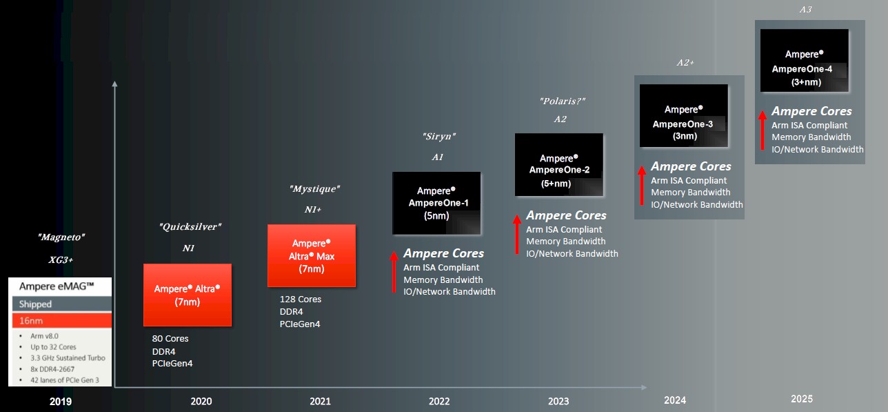
The performance data is a bit thin for the AmpereOne chip, but here is a one that shows how many single-socket servers you can cram into a 16.5 kilowatt rack and how many cores that gives you with the processors shown below:
In this case, threads are not treated like cores on the AMD and Intel chips. Which they should not be.
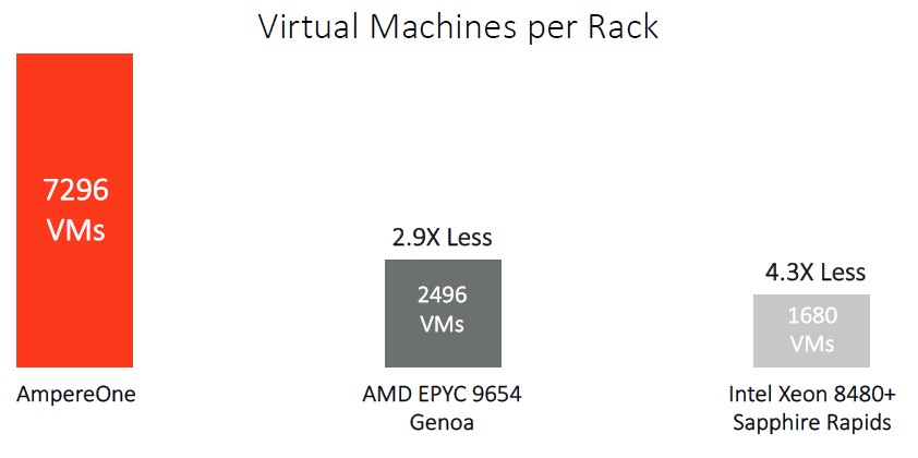
Wittich says that the AI experts that came to Ampere Computing through its OnSpecta acquisition back in August 2021 had a hand in the A1 core design, with the aim of providing high AI training performance. And here is how the Siryn AmpereOne with 160 cores stacks up against an AMD “Genoa” Epyc 9654 with 96 cores:
These performance metrics were measured at the rack level in 14 kilowatt racks.
We will get you the SKUs and more precise performance for the AmpereOne as soon as we can.

Intel’s Datacenter Business Goes From Bad To Worse, With Worst Still To Come
Everybody expected that Intel was going to turn in a pretty bad final quarter in 2022, and even before it posted its numbers yesterday after the market closed, there were plenty of signals that it was going to be worse. And it was. And the worst is still yet to …

AWS Goes Wide And Deep With Graviton3 Server Chip
It is always an exciting time when there is a new compute engine coming into the market, and interest is particularly keen with any new Arm server chip entry. At this point, Amazon Web Services is by far the biggest consumer of Arm-based server processors in the world, with its …

One On One With Jensen Huang: Nvidia, The Platform Company
While a lot of ideas are ancient, some are relatively new and can come from only a modern context. Platform is one such concept, and given what we care about here at The Next Platform, it bears some analysis as we consider the company the Jensen Huang, co-founder and chief …
VERY impressive. Note that Esperanto is shipping a RISC-V with over 1000 cores as well, although targeting a very different market. Thanks, TPM!
I’ll get to them!
Super cool
Respectfully though, 192 is divisible by 2, but it is not a “base 2” number any more than 179 or 333 is 🙂
Yup. Just moving too fast.
“The number 192 is significant because it is a base 2 number that is halfway between 128 and 256”
But 192 is not base 2.
2^7 = 128
2^8 = 256
log2(192) = 7.5849
Am I missing something on why you are calling it base 2? It seems wrong.
Multiple of 2, not base 2. Apologies.