

In a post Moore’s Law world, domain specific hardware is becoming more common. But getting a new compute engine into the field is not just about having the right design and manufacturing process. Money and timing inevitably play a role, at times hand in hand. If the timing isn’t right, the new money won’t be there to get the compute engine into production.
Franz-Josef Pfreundt, team lead for next-generation architectures for the Fraunhofer Institute for Industrial Mathematics, has seen how compute engines fail in the market, and recalls IBM’s “Cell” processor, which launched in 2007 and which was used by the institute. IBM abandoned the chip, which paired a brawny Power4 core and eight specialized vector engines, in 2010. (The Cell chips famously did most of the compute in the petaflops-busting “Roadrunner” supercomputer at Los Alamos National Laboratory.)
In the wake of Cell’s demise, Pfreundt partnered with Jens Kruger at Fraunhofer and Marty Deneroff at Berkeley National Laboratory to develop the GreenWave chip, a processor aimed at reverse time migration (RTM) workloads common in the oil and gas industry and also at accelerating climate simulations. The initial GreenWave chip was based on Tensilica cores, and the 28 nanometer design included 700 cores, 32 chips per node, an in-order core with scratchpad memory and solid performance. The Greenwave chip also came out in 2013 – too early for the industry and, therefore, with no money to produce it.
In 2016, Pfreundt and Kruger embarked on creating a new chip, teaming with ETH Zurich to design an accelerator that could meet the performance and efficiency demands for HPC and machine learning workloads. They didn’t chase a 5 nanometer design, instead looking to create a chip to do the work efficiently, both in power and cost.
“If you have a 5 nanometer design, you have to invest today half a billion dollars to get that,” Pfreundt tells The Next Platform. “That’s prohibitive for a small market. I always say cost is a matter of creativity. You have to think about good ideas and how to get there. We started to rethink this and rethink stenciled [processor design] in general and look for even the wider class of algorithms. We did the completely new core design, which has nothing to do with Tensilica or anything else. It was done from scratch.”
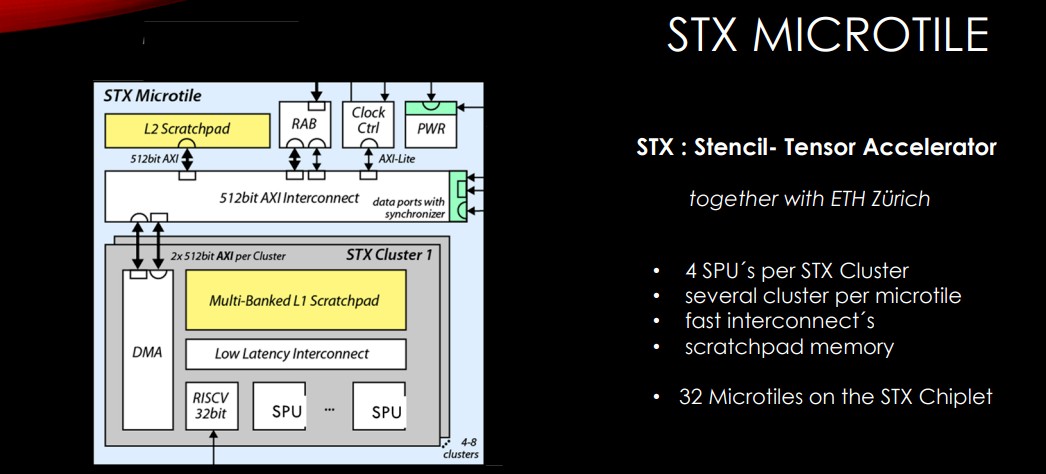
The result is the STX compute engine – that STX is short for stencil and tensor accelerator, which is part of the growing trend toward domain-specific processing – that tries to balance the conflicting demands for high power efficiency, easy programmability, and low costs. The STX chip was designed as part of the larger European Processor Initiative (EPI) that is driving the push for European independence in HPC and, eventually, exascale computing by relying more on EU-developed technologies.
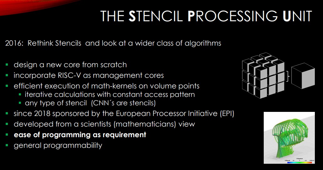
The EPI involves 28 organizations from 10 EU countries and, for Fraunhofer and ETH, provided the necessary funds. The effort late last year wrapped up its initial three-year phase, with chips ranging from general-purpose chips to memory silicon to accelerators, including STX.
The design includes a RISC-V processor as management cores for the accelerator. The STX is designed to execute “mass kernels on volume points,” Pfreundt says. “Every time you have a constant access pattern, which is any type of stencil with iterative calculation, that will work. One, for example, is wind energy. In the EPI, one side is this Arm processor which is being developed. Then there are the Spanish guys doing a RISC-V vector processor and we have this stencil processing unit, which in the first place is a specialized accelerator, but it will be general programming. This is the important point: It’s developed from a scientist’s view, so that makes programming easier and keeps the general programmability.”
The design includes a stenciling processing unit, or SPU, a small VLIW architecture with some key parts, including the address generation unit.
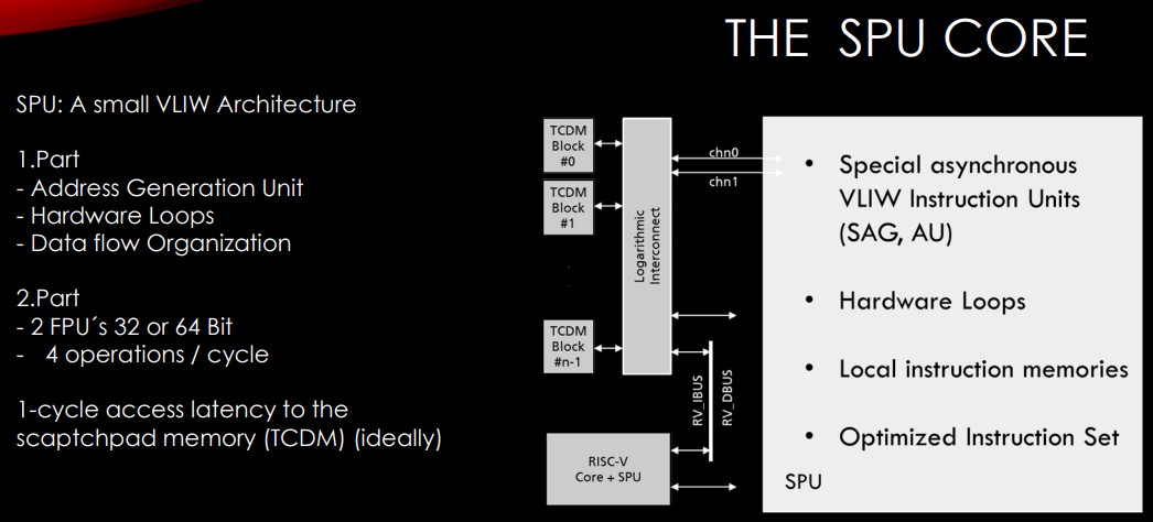
“When you imagine this large stencil, you have to do a lot of advanced calculations to get the points in memory where you have to get the data from,” Pfreundt says. “This is done in hardware. Since we have a constant access pattern within the loop, that means we can even put the looping in hardware. You run your loop index in hardware. This makes programming a lot easier. Sure, there are some ideas how to organize the data better. But this is the main thing and we have this scratch pad memory on the SPU as well.”
Having the address generation hardware reduces the overhead of chips that do so in software, Pfreundt says. It’s needed because users have a constant access pattern that isn’t modified and is always the same, so it makes sense to do it in hardware, similar to how it’s done in FPGAs.
There also are two floating point units (FPUs) that can be 32-bit or 64-bit and run four operations per cycle as well as the TCDM scratch pad memory. There are four SPUs – with a RISC-V management core – per cluster and several clusters per microtile and 32 microtiles per chiplet, along with scratch pad memory and a low-latency interconnect.
As for coding, developers can code formula as they would in C, C++, or Fortran, and the STX will work with that. That feeds into the push to make programming easier by avoid large porting and tuning efforts, he says.
“The compiler is really an essential piece and we spent a lot of time in the compiler technology,” Pfreundt says. “The compiler and the architecture are developed together so that the compiler guys really have an inference how the chip looks like and the other way around. Therefore, the code itself is simple enough that the compiler can do the job. It’s called a very large structural architecture, but actually the instruction was very short. There’s no vectorization that needs to be done at all, which makes life a lot simpler for a compiler. We have OpenMP support. It’s just one OpenMP call and code will compile. If we talk about the host, the host is a quad-core RISC-V core.”
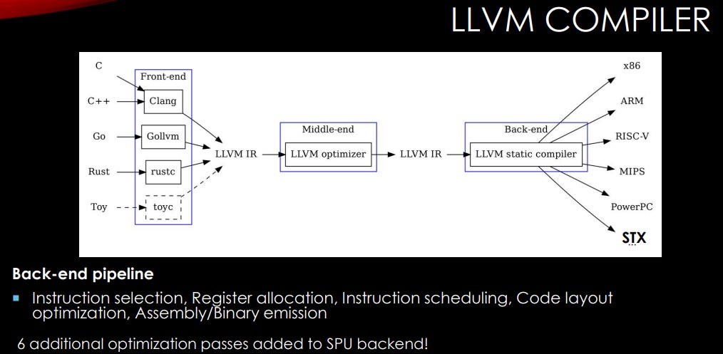
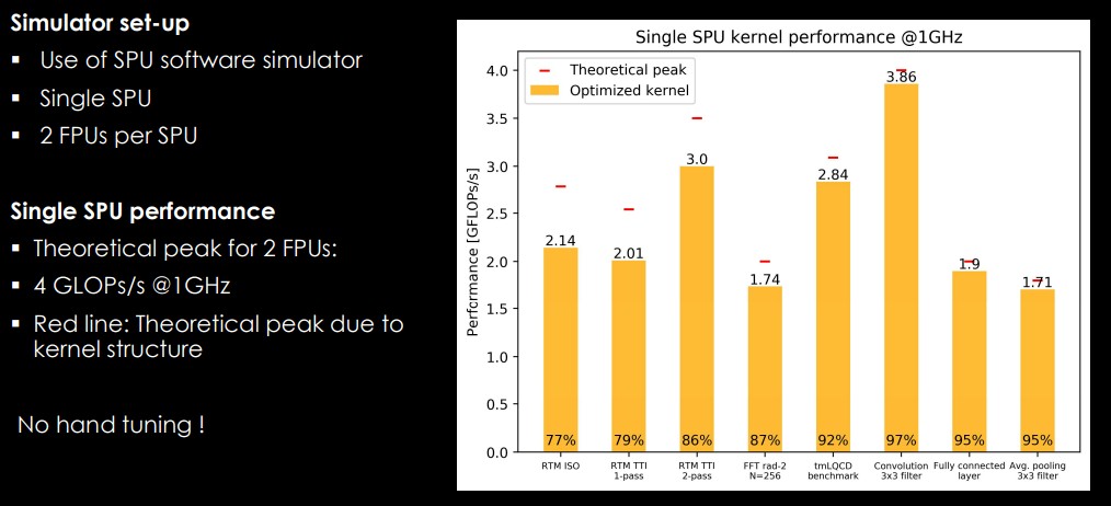
The design of the compiler enabled the developers to reach 80 percent of the theoretical peak performance, he says. It’s based on the LLVM architecture.
None of this was done on final hardware; instead, a software simulator was used to run tests of the SPU on a range of workloads, from RTM and fast-fourier transform (FFT) to convolutional neural networks and average pooling.
“What we see is that you have now many simulations which are combined with machine learning,” Pfreundt says. “They say in the fluid dynamics model, you have a machine learning that describes the turbulence model and so you’re very often have this combination now of machine learning with simulation and so we can do both in an optimal way.”
In addition, in tests two STX tiles show advantages in performance, efficiency, and cost when compared with Nvidia’s A100 GPUs. Two STX units are simulated to burn 70 watts and process 11,742 megastencils per second, for 152 megastencils per second per watt, compared to an A100 GPU, which burns 250 watts and does 13,000 megastencils per second, for 52 megastencils per second per watt.
Right now, the hardware setup is four SPUs per cluster and 128 clusters per chiplet, with clock speeds of 1.1 GHz, a 12 nanometer FinFET design, and 16 GB of HBM2e memory, with PCI-Express 5.0 CXL 2.0 support, and consuming 35 watts. It is manufactured by Globalfoundries, so it can be built in Europe, and Pfreundt says the STX chip helps drive down the cost by a factor of five what a GPU costs, he says.
In addition, Fraunhofer is a German company of 20,000 people, with 3,000 in microelectronics, including some who are specialists in design. It’s a nonprofit organization, so eventually it eventually will have to spin off the STX business to more quickly get it out to market.
The next steps in the process are working on the development of the next generation of STX, which will be sponsored by EPI, and further compiler development. The company also is pushing to productize it, including participating in a European pilot system. In the meantime, Fraunhofer also is talking with oil and gas companies that have shown interest in the accelerator, though Pfreundt declines to name any of them.


Europe’s Evolving View of “Continental Exascale”
Europe is known for taking its own routes in almost every segment and supercomputing is no different. While the broad expectation was for a Euro-centric processor ecosystem for exascale, that intention has been subverted in terms of hitting roadmap goals and establishing single-center dominance. Instead, Europe is taking a collective …
Atos Wins MareNostrum 5 Deal At Barcelona Supercomputing Center
UPDATED: The EuroHPC Joint Undertaking, which is steering the development and funding for pre-exascale and exascale supercomputing in the European Union, has had a busy week. The first phase of the 550 petaflops “Lumi” system at CSC in Finland was dedicated and opened for processing, and Germany’s Forschungszentrum Jülich has …
European Processor Initiative Readies Prototype
Europe is trailing the other major HPC powers in its quest to field exascale supercomputers. The first such European Union machines aren’t scheduled to come online until 2023, at which point the United States, China, and maybe even Japan are likely to have their initial systems up and running. But …
Mr. Burt,
Thank you for the fascinating, and quite informative, article. I noticed a few spelling/grammatical errors which are hurting the overall presentation, and would like to point them out below:
“on creating a new a new chip” –> remove one “a new”
“The STX is design to” –> designed
“but it will be general programing” –> programming (2 m’s)
“so that makes programing” –> programming (2 m’s)
“This makes programing a lot easier” –> programming (2 m’s)
“and run four operations per cyle” –> cycle
“It is manufactured by Globalfoundries” –> GlobalFoundries
Thanks, Joseph.