
There is a lot of chatter this week about optical communications with the OFC2022 conference being held in San Diego. We have more than a passing interest here at The Next Platform in silicon photonics and co-packaged optics, and had a chat with Andy Bechtolsheim about what was happening in these areas as it relates to the datacenter.
It’s like being able to ask Shakespeare to tell you what he really meant in Hamlet and getting to write a paper on that.
Bechtolsheim, of course, is the legendary systems and networking entrepreneur of Silicon Valley who was one of the co-founders of Sun Microsystems four decades ago and after a string of companies has been chairman and chief development officer of Arista Networks since it was founded in 2004. It is Bechtolsheim’s job to synthesize all of the networking requirements from hyperscaler, cloud, and now large enterprise customers, all of the switch and network interface ASICs that go into systems, and all of the research being done with electrical and optical signaling and try to plot a course for products for Arista Networks.
What follows is an interesting conversation on silicon photonics, and particularly the development of co-packed optics, which is trying to solve some pesky engineering problems but which may get beaten to the punch by other technologies if Bechtolsheim is correct.
Timothy Prickett Morgan: I understand there are different camps when it comes to silicon photonics and co-packaged optics. There are those who want lasers on the die and those who want lasers outside the die, and then there are those who want to co-package the optics and those who think pluggable optical modules, like we have been using for years now, are still going to be the best way to bring networking together with servers and storage. What are these camps, and what are the difficulties they are facing?
Andy Bechtolsheim: So I think the best way to think about this is that the goal is always power reduction. In other words, if there was no power reduction, nobody would talk about co-packaged optics. And obviously co-packaging is really a packaging technology – it’s not a new kind of optics, it’s not a new lambda, it’s not a new optical interface. It is actually is implementing existing IEEE optical industry standards, and in a way that, presumably, is driving lower power. That was the goal. If it did not offer lower power, nobody would mention it.
The power reduction that people had projected or imagined with co-packaged optics was at the 20 percent level compared to conventional pluggables.
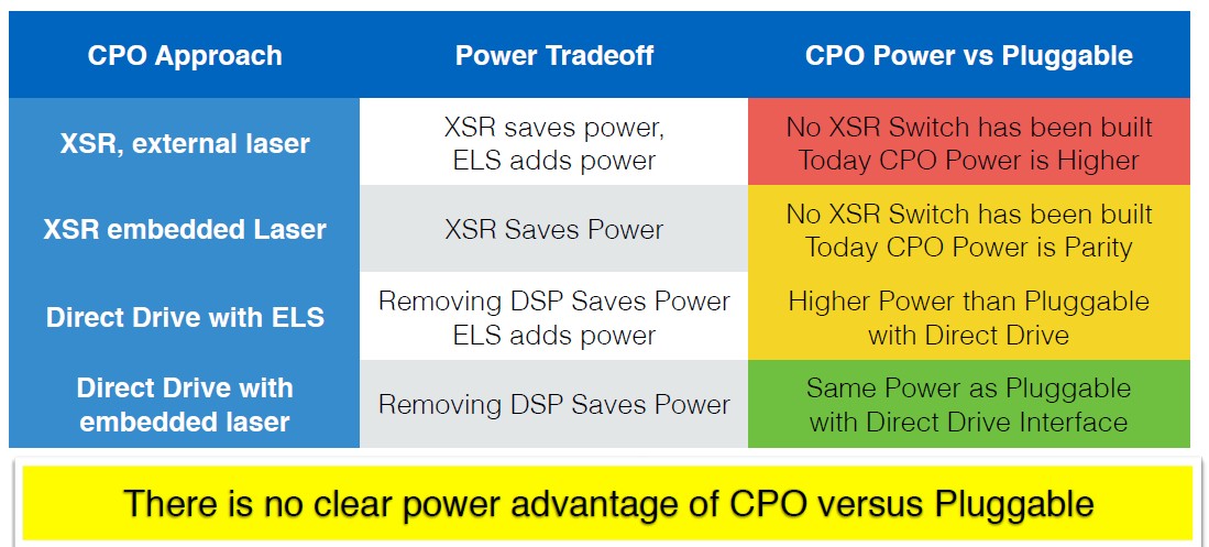
Now, when we now drill down on this power, one can categorize it into four major buckets. One is the electrical interface between the switch chip and the optics, which of course, if you make it shorter, you need less power, and that’s good. The second one is the DSP chip, which doesn’t really change because it is driven by the optical requirements. Then there is the laser power and the optical modulator. All of these add up to the total power.
Co-packaging reduces the electrical channel lengths, and if you have what is known as an XSR channel, which is an ultra-low power channel with a few centimeters of reach compared to a VSR channel, which has the ability to drive a signal over ten inches, you do save power there. But nobody ever built a switch chip that has an XSR channel because there is no market for it. It is a very expensive tape out, and people are not going to do it unless they can get a return on investment. So, as of today, there are no switch chips that have XSR channels, and the XSR will only be relevant when there is silicon customized for that interface.
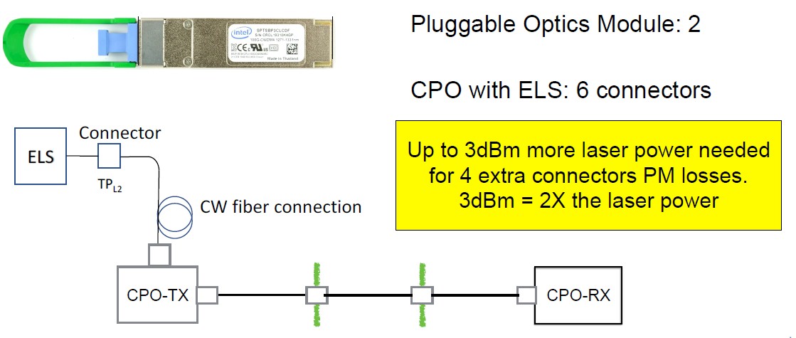
On the optical side, most approaches except for Intel have an external laser source. And the external light source is connectorized, meaning it’s a blind mate fiber connector that connects to the co-package on the chip and then there is another connector from the co-packaged chip to the front panel. So you have four additional connectors in the link compared to pluggable optics. In addition, there are splitters for the external light source to be divided into the channels, and then there is the whole problem with polarizing fiber, which is never quite perfect, resulting in some additional losses.
TPM: You know, you are making this sound a lot less fun than I thought it would be. But continue.
Andy Bechtolsheim: [Laughter] The difference in optical efficiency with an external light source is 3 decibels – so you need 3 dB more laser light to achieve the same 0 dB output on the interface that is required by the IEEE spec. And 3 dB on a laser is doubling the laser power. you are actually burning a lot more energy, and this laser is only like 10 percent efficient at high temperatures. So you’re burning a fair amount of additional energy to drive an external light source to produce the same optical output as a pluggable module. And as a result, today co-packaging is actually higher power than pluggables because of this extra laser power required.
In fact, the laser impact is quite significant. And because in the worst cases the switch is at a high temperature and people talking about 500 milliwatt lasers, which are really running quite hot and they will have an electrical input of over 10 watts. So it is a very heavy duty laser and there are potential safety issues as well as the fact that if the connector gets contaminated with any kind of dust particles that may melt the glass tip of that fiber.
TPM: This doesn’t sound much like a reduction in power, which at the very least means it will not be attractive to the hyperscalers and cloud builders who want power per bit moved and cost per bit moved to go down every generation. So how is that power going to come down as the bandwidth goes up on switches?
Andy Bechtolsheim: If we look at how to reduce power, there are very promising new optics modulation technologies compared to silicon photonics.
The history of co-packaging is closely related to and coupled with silicon photonics because you need an efficient manufacturing technology to put 16 channels or 32 channels on a single chip. In the legacy world, when people have built these things in foundries, they would not have yielded. But arguably, with good silicon photonics, like Intel and others have demonstrated, you can do it.
However, silicon photonics has one big problem, which is that it is a high insertion loss modulator. You need an enormous amount of laser power to make up for the fact that you’re going to lose roughly 15 dB between the laser and the way out. So to reduce power, the best technology is actually not silicon photonics, but newer technologies, including thin film lithium niobate and barium titanate, and there are others doing organic modulators and even graphene modulators.
So there are four quality and quite promising technologies on the horizon that use different optical effects to achieve the modulation. And they do it at much lower voltage levels, so there is less driver current; they have much less capacitance, so you need less energy, and you get higher bandwidth. Basically, all of these new things that are on the horizon are lower power than silicon photonics modulators. Silicon photonics modulators are a cost effective, highly manufacturable technology. However, they are not low power. And people really want to address the power issue, so you have to bite into the apple and see there is an opportunity for new technology.

At Arista, we actually have worked with some key suppliers to build a lithium niobate thin film pluggable module at 800 Gb/sec using eight channel 112G per lambda, which us done with a 7 nanometer DSP.
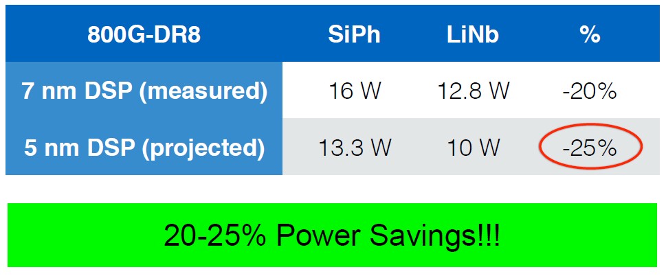
The competing silicon photonics products are in the 16 watt range today, and the lithium niobate with the same DSP is at 12.8 watts. Call it a 3 watts savings. With a 5 nanometer DSP, we expect the regular silicon photonics to come down to 13.3 watts, a savings of 2.7 watts, but the lithium niobate will be at 10 watts. That is an incredible power reduction, and it is actually now at the power level of what the co-packaged optics people wanting to achieve just by fixing the modulator insertion loss.
This kind of improvement, unfortunately, is a lot harder with co-packaging because the lithium niobate modulator is a lot bigger than silicon rings. And as a result, it doesn’t quite fit so well on a co-package slice. And this is not a problem with the module – there is plenty of area there – but putting 32 of these channels in the OIF-defined form factor with a DSP is going to be quite challenging, let’s just say. In addition, Lithium-Niobate is not silicon photonics, so there may be other yield issues that have to still be resolved.
Now, there are other promising things on the horizon. The BTO modulator I mentioned above will have even lower insertion loss and it has a higher efficacy in terms of converting electrical energy to the desired optical effect of modulation. So perhaps they can get to even lower power levels. They had some promising early demos in the lab, but there’s no complete module yet that would allow us to measure it; we will have that later this year or certainly early next year. And the organic module people claim even more efficiency and even lower power, but again, this is still at the lab stage. The lithium niobate modulator is still a prototype and it may take 18 months or whatever to get to volume.
Predictably, I think there will be a high interest in these new modulation technologies because it’s the easiest way to get the power down. It’s a change in physics on the modulation path, which then helps to reduce the laser power, which by the way also makes the laser more reliable because the easiest way to make the laser more reliable is to reduce the power, which reduces the heat, which reduce the thermal problems. And that’s why we think that the most promising action for the industry right now is to just focus on lower power modulation.
But here is the real issue that co-packaged optics is facing compared to the pluggable transceiver world. In the pluggable world, the choice of the optics technology is not tightly coupled to the switch chip. They are disaggregated and you can deliver a pluggable module to the market and insert into a platform that shipping in high volume whenever it’s ready.
In a co-packaging world, you pretty much have to make the choice of what technology you are going to bet on two years in advance. It takes that long to develop these 32 channel slices, and it gives them a chance to iterate and it requires you to spec on Day One. So if you want to do co-packaging today for a 102.4 Tb/sec switch chip coming in 2024, you have to start right now, making commitments the exact design of that, that co-package optic slice. Whereas with pluggable optics, you’re completely decoupled, and if it takes us a year or longer to get it ready, it’s no problem, we can ship that in 2025.
TPM: It is always hard to bet against disaggregated components. In all levels of the system, we need to decouple specific technologies so one delay doesn’t halt everything and yet have deep and open interconnects so we can attach anything to anything within a socket, within a node, or across a network.
Andy Bechtolsheim: From a business level, you have all the competition in the current supply chain. There are many companies making these pluggable optics modules, you can also have competition in the new technology space, because the company that is betting on barium titanate modulators is not going to bet on lithium niobate. One will succeed better than the other, but it is too early to tell. I couldn’t tell you. And if you talk to these startups, they are wildly optimistic, they got the best thing since sliced cheese.
TPM: And another will say they have the next best thing since sliced white bread, and we can make little sandwiches. . . .
Andy Bechtolsheim: [Laughter] Right. On a lab basis, they all have valid points. But none of them are in production, which means millions of units. In the end, if you can’t make it the millions, it’s not a solution for the market because they couldn’t ramp it.
TPM: I understand that lowering the power and lowering the cost per bit moved are the driving forces for the hyperscalers and the cloud builders, but are there times when they will accept higher power on network devices – switches, optics, or network interface cards – in exchange for lower capital costs?
Andy Bechtolsheim: There are customers who only care about cost. The truth is, it is happening today. Today, with the optics power, the difference is like a 20 percent to 25 percent savings at the optics component level or the module level, but at the level of the datacenter, this is 1 percent or lower. Out of the total power, including servers and storage and switches, the optics are just not that big of a driver.
However, on a per rack basis or per datacenter facility room where they have a limited power capacity per room and per rack, the customer doesn’t have a choice and cannot change the datacenter because it was just built five years ago or whatever and at the time they might have provisioned, say, two kilowatts per rack. So they always have to keep the power down because they are boxed in. So there is a physical constraint on power, which is unrelated to, you know, green energy or saving the climate, and changing the optics can make a contribution there, of course. And some people may be willing to pay a premium because the new technologies that allow lower power may cost a little more initially.
In terms of high-level goals for networking, lower power is desirable. Cost is sort of a separate issue, but people want low cost, low power and high reliability, but as I said, the low power goes hand in hand with high reliability because lower laser power has been proven to be the best way to increase laser reliability. Ignoring dust contamination, 90 percent to 95 percent of optics failures are due to lasers, and that data is for 100 Gb/sec transceivers, and it will get worse at 400 Gb/sec because the lasers are hotter. The laser is the culprit here. But if you create a laser that uses 1/10th the power, its reliability goes up by many orders of magnitude.
I think the crux of this whole argument is that people want highly availability, they want low power, they want high bandwidth, but the hardest one is reliability. And focusing in on reliability, there is a serviceability aspect. With pluggable modules, it is easy: you pull it out and replace it in the field while the switch is running. With co-packaging, if there’s a switch-level failure, it’s a very expensive replacement, though the external laser source (ELS) is pluggable, which addresses a part of that. But there is still 5 percent of the optics failures that are not ELS related – and that is only one of them. If you have 64 or 128 of them in your system, they could dominate the number of fields events. This is not a happy thing, because we don’t want to get a switch back because something in the optics fails.
TPM: What bets are the hyperscalers and cloud builders making with regard to optical transceivers and co-packaged optics in the network? Are they different or do they all track?
Andy Bechtolsheim: They’re not really all that different, meaning everybody wants this high reliability and lower cost.
Oh, by the way, there is one issue we need to discuss before we get to the goals here. And that is that network costs are highly related to volume. Meaning all of these things have significant upfront engineering expenses, product costs, capital costs equipment to put this into production. Without volume, co-packaging will never be more cost effective than pluggables. In the pluggables world, the industry is making 10 million optical transceivers a year, and co-packaging is starting at zero and it will take a long time to move up.
And then you have this you know mix and match issue, and co-packaging really only works with the same optics standard interface for all the ports on the switch. You can’t mix and match transceivers as you can with the pluggables.
So the question is: Will co-packaged optics ever get to volume because you can only get volume if it’s proven, ultimately, that is reliable, manufacturable, and cost effective. If it was cheaper, people would pay attention, right? But today, it’s not cheaper. It will take significant volume to get cheaper.
TPM: They have the classic chick-and-egg problem, there. And if there were no engineering tricks on the horizon – you know, four years ago, a lot of people, including you, said that electrical signaling would run out of gas at 112 Gb/sec native signaling, and here we now have some material science progress and it looks like the industry will be able to push up to 224 Gb/sec native signaling.
Andy Bechtolsheim: While it is true that four years ago I had projected that it would be quite challenging to go beyond 100Gb/sec SerDes electrical speed, it has become clear now this is not only feasible, but will happen in the 2025 timeframe and is not the inflection point that would lead to the adoption of co-packaged optics.
But there is a second issue here as it relates to external lasers and particularly with the ring modulator technology from Ayar Labs, which is optimal at slower speeds, that is, 32 Gb/sec and 64 Gb/sec using NRZ encoding. It may reach 112G-PAM4, but my understanding is that it cannot easily support 224G-PAM4, meaning that Ayar’s technology, by itself, cannot fix the high-speed I/O problem. There is, of course, always the possibility of using inverse gearboxes to go down from 224 Gb/sec to 112 Gb/sec, but inverse gearboxes are not power or cost efficient, and in any event do not increase how much I/O one can get off a chip.
Broadcom claims a 50 percent savings for co-packaged optics, which is based on eliminating the optics DSP and using the switch SerDes to drive the optics directly. This is true, however you can do this also with pluggable modules and a suitable switch SerDes.
Our firm conclusion is that co-packaged optics is not necessary for 224 Gb/sec signaling. So at this point, there is nothing driving co-packaged optics except this perception that it was going to be lower power. But you can get to lower power much more easily just by changing the modulation technology.

Gelsinger Leads Emboldened Intel With Ice Lake Launch
The past several years haven’t been easy on Intel. The world’s top processor maker stumbled on its transition from 14 nanometer to 10 nanometer manufacturing and still finds itself behind rivals like AMD and Arm, which have made the move to 7 nanometer processes and which have line of sight …

AMD Finally Breaks The 10 Percent Server Share Barrier
History doesn’t really repeat itself, but it surely does use a lot of synonyms and rhymes, and sometimes, if you listen very closely, you can catch it muttering to itself. It is with this in mind that we contemplate the recent data coming out of Mercury Research, which is the …

Why Memory Enclaves Are The Foundation Of Confidential Computing
Sponsored Feature There are tens of millions of lines of code in thousands of software programs, on a typical server in the datacenter. All of which collectively present a huge attack surface for various kinds of malware. And no matter how hard vendors and open-source project developers try to secure …
This is all viewed from longer distance (ethernet) communication (what Arista is doing) point of view, but what about using silicon photonics/co-packageing for inter (chip) package communication ? It looks like lots of things AB is mentioning are not necessarily negative any more like the Ayer Labs >112G problems (just more lambdas could be a solution for speed and power) and laser efficiency loss. Also EMIB and other chiplet interconnect tech can minimize/decouple development and production time constraints…
As mentioned above but not talk in depth, we should separate the power saving target into two aspects: first, electrical side, second optical side. in electrical side, the right way is to reduce the trace length if we don’t develop a revolutionary PCB material. reducing the trace length so that you don’t need DSP in optical side or you just need a very light equalization, thus you save half of the power dissipation in optical side compared to pluggable, either eml, siph, or the new Lithium thin film modulator. same way to receiver side. in optical side, the industry just needs to do right thing to get optical power dissipation dropped, not just stick to pluggable which can’t solve the high speed signal integrity by long trace at all. For example, using MRM instead of M-Z interferometer, or try to see if LiNbo3 thin film over silicon/silica could be integrated by arrays.
DSP itself is not just power saving, if you use 3nm, it still needs to compensate the signal impairment. the cost increases. so pluggable doesn’t help at all.
DSP also affects the latency, normally a DSP has ~200ns latency round trip. if in next generation of 200G PAM4/lane, you have to put a canscaded FEC there, you may have over 400ns latency again, this is somewhat unacceptable in AI/ML. you may argue that pluggable could also be direct drive, maybe someone reported this, while it needs strong driving and equalization by more taps, it doesn’t solve the real issue that is introduced by long trace length, so power and latency issue can’t be saved by DD pluggable.