
When it comes to memory for compute engines, FPGAs – or rather what we have started calling hybrid FPGAs because they have all kinds of hard coded logic as well as the FPGA programmable logic on a single package – have the broadest selection of memory types of any kind of device out there. And the new Agilex-M series just announced by Intel might have the most options we have ever seen.
The question is, just how useful is all of this memory and how can programmers seamlessly take advantage of it without gutting their applications?
Before we get into that, let’s drill down into the Agilex-M devices, which are a follow-on to the Stratix 10 MX hybrid FPGA, which came out way back in December 2017 and which has subsequently been fleshed out with the Stratix 10 NX that debuted in November 2020 tuned for AI inference workloads and with HBM memory, and the Stratix 10 SX line from August 2019, which did not have an HBM option.
The high bandwidth memory and its close proximity to programmable logic compute, all in a single package, means that machine learning inference and various kinds of signal processing workloads can have extreme low latency – which is one reason, other than the programmable nature of FPGA, why these hybrid FPGA devices still exist in the compute engine arsenal. The fatter DDR5 and Optane 3D XPoint memories that complement the SRAM co-located with the programmable logic, are an object lesson in hierarchical memory for systems.
In many cases, the continual stepping up of bandwidth on the network uses to interchange data is driving the compute and memory bandwidth needs on the devices. As more data is moved faster around the datacenter to various applications at higher and higher rates, the speed of the memory to keep feeding CPU, FPGA, GPU, or DSP engines is becoming a bottleneck, and hence the adoption of HBM memory in a slew of CPUs and FPGAs after it was first deployed with GPU accelerators some years ago.
The feature image above gives you a generic feel of what the Agilex-M device looks like, but this block diagram is actually more accurate:

As the block diagram shows, there are actually two stacks of HBM2e memory, each with DRAM stacks up to four or eight 2 GB chips high. If you use four stacks across the two HBM2e memory ports linked to the compute complex by EMIB links, you get 16 GB; if you go with the eight high stacks, you get 32 GB. It is a wonder that Intel did not push it to 64 GB of HBM2e capacity, but apparently the sweet spot for this level of device is 32 GB. Each HBM2e stack has eight channels and delivers 410 GB/sec of bandwidth, for a maximum of 820 GB/sec for the full device.
But that is not all for memory bandwidth because the Agilex-M also sports DDR5 memory controllers which can drive up to eight DDR5 memory sticks (presumably that is four DDR5 controllers), adding another 315 GB/sec of bandwidth. Intel is not clear what the capacity of this DDR5 memory can be in any of the presentations or spec sheets we have seen, but if you assume that 32 GB or 64 GB is the norm that people will pay for, then it should be an additional 256 GB or 512 GB of fat but slower memory. The DDR5 memory (Intel’s benchmarks show it using 32 GB memory sticks) would be 8X to 16X times as fat, but would be a factor of 3.6X slower in terms of bandwidth. If customers need even more slow memory capacity, then they can opt for Optane Pmem modules, which plug into the DDR5 slots (which are backwards compatible with DDR4 memory) and Intel’s Optane 200 series memory is available in 128 GB, 256 GB, and 512 GB capacities. So the Agilex-M could have 16 GB to 32 GB of very fast HBM2e memory, a few hundred gigabytes of slower DDR5 memory, and up to terabytes of even slower (but still pretty fast) Optane Pmem, all on the same device.
By the way, there are two network-on-chip (NoC) hard blocks for access to the off-chip HBM2e, DDR5, and Optane memories – one on the top and one on the bottom. These NoCs have a combined bandwidth of 7.52 Tbit/sec, which is used to pump data from the external memory into the memory embedded in the programmable logic.
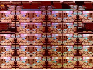
But wait, that is not all you get. Don’t forget that on-logic memory, the MLAB blocks and M20K block RAMs that sit right on the programmable logic fabric. Here is how the programmable logic and memory stack up on the two SKUs offered in the Agilex-M series:
The AGM 032 part has 311 Mb of M20K memory and 33 Mb of MLAB memory against 3.25 million logical elements, and its programmable DSP blocks deliver 14 teraflops at FP32 single precision and 28 teraflops at F16 half precision. The AGM 039 part, which presumably has close to all of the programmable logic fired up – it all depends on the yield Intel is getting with its Intel 7 process, formerly known as 10 nanometer SuperFIN – has 370 Mb of M20K memory blocks and 40 Mb of MLAB memory against 3.85 million logic elements. This beefier chip delivers 16 teraflops at FP32 precision and 32 teraflops at FP16 precision. That is not the performance level that AMD – and soon Intel and Nvidia – is seeing with its GPU motors. AMD’s “Aldebaran” Instinct MI250X has 47.9 teraflops in its vector engines for FP64 and FP32 (for both) and 95.7 teraflops for FP64 and FP32 for its matrix engines. On those same matrix engines, the FP16 and BF16 performance is 383 teraflops. Intel’s “Ponte Vecchio” Xe HPC GPU accelerator is expected to deliver at least 45 teraflops at FP64 and FP32, and somewhere around 312 teraflops at BF16 precision.
The performance gaps are obviously quite large, and so the use cases in the datacenter and at the edge for CPUs, GPUs, and FPGAs are going to come down to history, compute engine availability, cost, watts, and other factors such as the need for programmability (particularly out in the field).
As far as Intel is concerned, the Agilex-M needed to stand toe-to-toe with the Xilinx Versal HBM device, which will start sampling in the first half of this year, and it does as far as Intel can tell. The Versal HBM device has 1,081 GB/sec of memory bandwidth out of its HBM2 banks, which weigh in at 8 GB, 16 GB, and 32 GB capacities and deliver 819.2 GB/sec of bandwidth. (The Achronix Speedster 7t FPGA has a memory bandwidth of 512 GB/sec, by comparison, using GDDR6 memory.) The Agilex-M will crest at 18.45 teraflops at FP32 and 88.6 teraops at INT8 (important for lower precision inference), and this can be dialed all the way down to INT1 if need be on the programmable logic. The Versal HBM device from Xilinx (now part of AMD, of course), is a little bit less capacious on the math, at 17.5 teraflops at FP32 and 74.9 teraops at INT8. But these two devices are within spitting distance.
Which leaves us with a few questions, for which we do not have easy answers. First, the widening memory hierarchy that Intel is putting out there with the Agilex-M is interesting, but it could be a bear to program. (Then again, coding FPGAs is already tough, so what is a few more twists and turns?) But the benefits could outweigh the programming issues. Intel seems to think, as expressed in this white paper, that various kinds of stencil programs in the HPC space, such as oil and gas reservoir modeling, weather and climate modeling, and thermodynamics, could be accelerated by FPGA hybrids. Intel’s solution brief on the Agilex-M shows it being used in firewall in conjunction with Xeon and other SoCs, like this:

Intel also thinks that the Agilex-M can be used to support 4K ultrahigh definition (UHD) video streaming and be able to use the same iron, with some reconfiguration of the programmable logic, to support 8K video. There are also the usual suspects of AI inference, various kinds of network processing (meaning communications network, not neural network), and, yes, you guessed it, cryptocurrency mining. But didn’t Intel just reveal its plans for the “Bonanza Mine” cryptomining ASIC, you say? Yes, indeed Intel did. Intel has five chips for every job, and the choice matrix is very hard to balance across the compute engines and out through the roadmaps and supply chains in moneyspacetime.
Neither Intel and now AMD is very clear about what FPGAs cost, and AMD, Nvidia, and Intel are presumably not going to do any better with their future GPUs, either. At least we can see list prices for CPUs still, which provides a ceiling on costs but never a floor.
What we can honestly say is that ramping FPGA volumes with expanding use cases can help drive down costs and push roadmaps. So a cryptomining use case, for instance, could help make AI inference on FPGAs cheaper over the long haul. This is why we care.
Xilinx will be sampling the Versal HBM sometime in the first half, and Intel will be sampling the Agilex-M by the end of the year. Compute engine buyers have lots of time to figure out what they might do with these HBM-juiced FPGA hybrids. And if everything ends up speaking data parallel C++ thanks to oneAPI at Intel, and some sort of hybrid ROCm/Vitis at AMD, maybe customers will get in the habit of coding one time and testing on all kinds of compute engines with the same code to weigh price, performance, thermals, and availability to see what engine they should pick – and when. The current revenue distribution for CPUs, GPUs, and FPGAs in the datacenter is probably a reasonable proxy for what the future distribution will be in a few years. We don’t expect dramatic changes in position because all of these compute engines are being re-engineered at a continuous pace along the same Moore’s Law curves – more or less.
As for wrestling with the memory hierarchy, FPGA developers have been doing this for a long time, and they are well-versed in dataflow programming. So we think they can handle a few more layers of fatter and faster capacity. They may, in fact, be the only group of programmers in the world who can. Everyone else may have to just choose a memory type for their compute engine and be done with it to simplify their programming models.


With Cloud HPC Toolkit, Google Pursues HPC, Intel Pushes OneAPI
The people running Google Cloud can see the tides of HPC changing and know that, as we discussed only a few months ago, there is a fairly good chance that more HPC workloads will move to cloud builders over time as their sheer scale increasingly dictates future chip and system …
Ladies And Gentlemen, Start Your Compute Engines
We have a bad case of the silicon shakes and a worsening deficiency in iron here at The Next Platform, but the good news is that new CPU processors from AMD and Intel are imminent, and more processors are expected later this year from IBM and Ampere Computing, too. There …
Intel Fills In The First Half Server Pothole – And Then Some
Let’s face it. Given how poorly the server market was doing in the final quarter of 2018 and the first two quarters of 2019, we had no idea how well or poorly 2019 might end up for Intel’s Data Center Group and the server industry at large. As it turns …
Be the first to comment