

When the hyperscalers, the major datacenter compute engine suppliers, and the three remaining foundries with advanced node manufacturing capabilities launch a standard together on Day One, this is an unusual, significant, and pleasant surprise. And this is precisely what has happened with Universal Chiplet Interconnect Express.
The PCI-Express interconnect standard and its predecessors have defined how peripherals hook into compute complexes for decades, and thankfully after a long drought of seven years getting to 16 Gb/sec data rates with PCI-Express 4.0, which spec’d out in early 2017 and first appeared in systems in late 2018, the PCI-Express standard looks like it can carry us to the end of the decade with a doubling of bandwidth every two years. This, of course, is a cadence that matches the Moore’s Law improvements in transistor density and throughput for compute engines of all kinds, which is why it is natural enough to look inwards and start using PCI-Express as the basis of a chiplet interconnect.
That, in short, is precisely what UCI-Express is going to attempt to do, and not a moment too soon with every compute and networking chip vendor looking at 2D, 2.5D, and 3D chiplet architectures as they snap their chips into pieces to make them more manufacturable at an economic cost as Moore’s Law slows down but performance and throughput demands on compute and networking devices rising faster than the thermal envelopes.
Make no mistake about it. If the engineers who worked on electrical signaling had not had some breakthroughs in recent years, and confidence that they can keep pushing materials science to the limits and deliver PCI-Express 6.0 and 7.0 with high confidence and with a line on PCI-Express 8.0 through 10.0 running out to first deliveries maybe in 2030, there would not be a chance to have a universal chiplet interconnect at all. We would be looking at a free-for-all for intra-socket communication, and that would clearly stifle innovation. (More on what this could mean in a second.)
It is the relative predictability of the PCI-Express roadmap – which frankly was not pushed hard enough before Intel was perfectly happy to sell processors that were I/O bound for many years and other compute engine vendors, who have smaller volumes, had little choice but to invent their own faster interconnects – as AMD, IBM, Nvidia, the Arm collective, and others had done – to link their ASICs to other devices.
Sometimes these links looked more like NUMA interconnects, such as IBM’s “BlueLink” OpenCAPI protocol or Nvidia’s NVLink, sometimes they looked like glorified PCI-Express, such as the CCIX protocol promoted by Xilinx and then the Arm collective. Sometimes they were somewhere in between, such as with AMD’s Infinity Fabric, which is used to link compute and I/O chiplets inside of a socket and which is also used to connect CPUs to each other, GPUs to each other, and CPUs to GPUs in shared memory system. (To one way of thinking, Infinity Fabric is a superset of PCI-Express that has some of the shared memory goodness of AMD’s HyperTransport (HT) thrown in, and to a certain extent, we can think of Intel’s Compute Express Link (CXL) as a kind of PCI-Express gussied up with some UltraPath Interconnect (UPI) memory semantics strapped on.) Intel was also working on the Advanced Interface Bus, a royalty-free PHY for connecting chiplets that was announced in 2018, and a few years before that the Open Compute Project launched its is Open Domain Specific Architecture effort, which did not garner a lot of support. (In 2020, Intel donated AIB to the Chips Alliance, which is when AIB v2 was also announced.)
As we are fond of pointing out, if InfiniBand had fulfilled its original promise from the late 1990s, we would have been talking maybe five years ago about InfiniChip or something like that inside of the socket gluing together chiplets. But InfiniBand, which was supposed to be a universal interconnect replacing PCI, was relegated by the dot-com bust to being a high-end HPC interconnect and a much less impressive (at the time in 2003) PCI-Express bus was created to extend PCI and PCI-X into the future. And excepting that seven-year bandwidth drought getting to PCI-Express 4.0, it has worked pretty well. And when the industry all got behind CXL as the accelerator and shared memory protocol to ride atop PCI-Express, nullifying a some of the work that was being done with OpenCAPI, Gen-Z, NVLink, and CCIX on various compute engines, we could all sense the possibilities despite some of the compromises that were made.
Debendra Das Sharma, Intel Fellow and director of I/O technology and standards at Intel, talked about the possibilities with CXL last summer at the Hot Interconnects 28 conference, which we covered in detail here. (For our deep dive on CXL, which we are not getting into here, check out this link.) Das Sharma talked about the obvious asynchronous but cache coherent links between CPUs and network interfaces and DPUs as well as to compute accelerators that have their own memories, and even shows that adjunct memory buffers could use CXL to add what is essentially a memory socket to CPU complexes. And following in the footsteps of IBM with its Power9’ (a rev of the Power9 chip that was never commercialized) and now Power10 chip (which started shipping last fall), which use generic SerDes to drive memory and I/O instead of dedicated DDR memory controllers, Das Sharma even indicated that in the future, we could see PCI-Express PHYs that were fast enough that they could replace DDR controllers and use CXL as a memory driver. One intrepid reader pointed out what we were thinking at the time, which was that CXL might be a good CPU-to-CPU interconnect, and therefore also possibly a chiplet interconnect. Why not? AMD shows this is perfectly doable with Infinity Fabric with 2D packaging.

It is no surprise to us at all that the UCI-Express protocol is coming out of Intel’s Beaverton, Oregon facility and that Das Sharma is driving it and the author of the whitepaper describing its goals. And given that Intel Foundry Services wants to open itself up to manufacturing all kinds of chippery and the packages (direct ball grid array mounted or socket) that wrap around them, it is no surprise, either, that Intel wants an open chiplet standard. This will be a necessary condition for the mass customization and co-design that is going to be necessary for all kinds of compute and networking as Moore’s Law transistor densities increase but the cost per transistor does not necessarily go down.
The costs for making an advanced chip are already exploding, and making a big, fat device is already a game for only the rich:
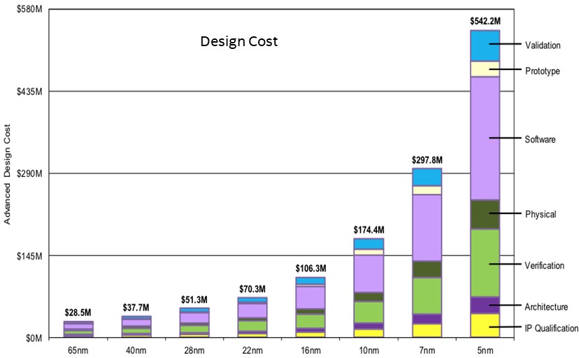
Moving to chiplets is a way to help lower the manufacturing costs and increase the yields on packages, but there is an increasing cost in package manufacturing and more complex testing and validation. It would be interesting to see the data for the above broken out by monolithic and chiplet designs.
As Das Sharma points out in the whitepaper, UCI-Express is not just about having the ability to mix and match chiplets with different designs from different designers, which is a powerful concept indeed. (Imagine being able to make a package with a baby Xilinx programmable logic block, a set of AMD Epyc compute blocks, Intel CXL memory and I/O interconnect, and Nvidia GPU chiplets?) The other key driver of the UCI-Express standard – and why it needs to be a standard – is to create well-defined die-to-die standards and testing and validation procedures that mean mixed-and-matched chips work when they are assembled into a 2D socket complex or a 2.5D interposer complex.
The UCI-Express 1.0 specification covers those two use cases, as shown here:
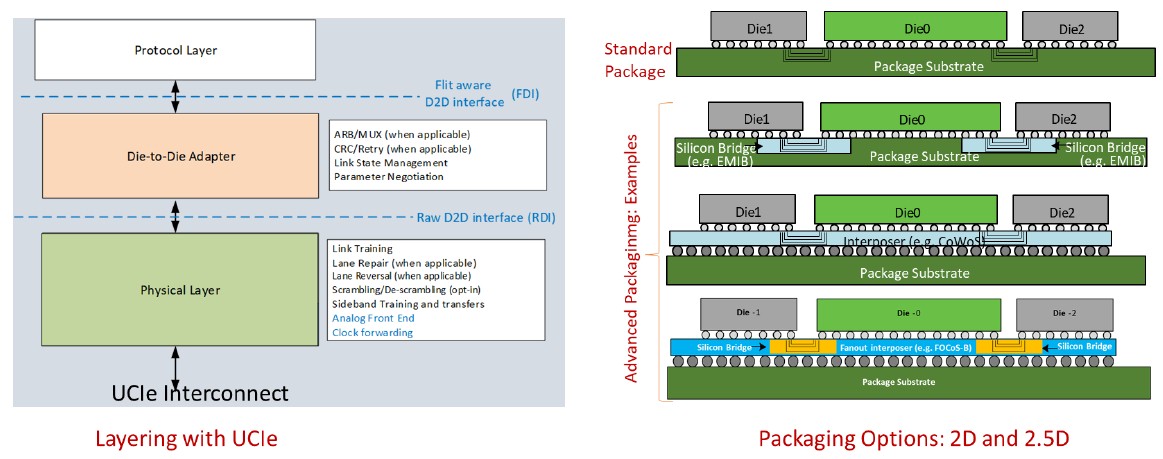
It is interesting to contemplate how UCI-Express will allow components of the server motherboard of today to be brought down into the package or socket of tomorrow as well as being used to interconnect compute and networking elements inside of that package or socket. And with the addition of a UCI-Express switch – why not? – either on the package or on the motherboard, there are all kinds of interesting, fine-grained interconnect possibilities that could span several racks and with optical links could span rows in a datacenter. Imagine if any element within a compute complex to talk directly over a PCI-Express fabric in a few hops to any other element within a pod of gear, without InfiniBand or Ethernet with RDMA? Just get rid of it all, and talk directly. This is why we have said that PCI-Express is the unintended by formidable datacenter interconnect and that across a datacenter with the need for peer-to-peer links to all kinds of components, PCI-Express fabrics will be pervasive.
To make sure there is the widest degree of interoperability, the UCI-Express specification supports different bump pitches, channel reaches, lane widths, and data rates, as shown in the table below:
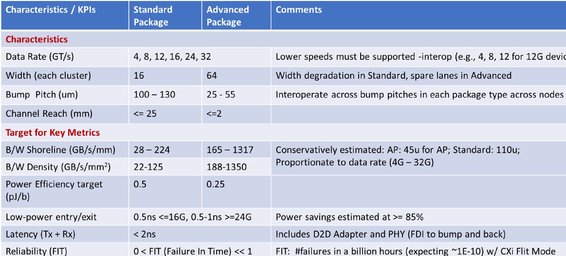
Das Sharma explains how this all comes together in two packaging options, which are called standard and advanced as shown in the table above, thus:
“A die with the standard package design is expected to interop with any other design on the standard package. Similarly, a die with the advanced package design will interoperate with any other die designed for the advanced package, even within the wide range of bump pitch from 25u to 55u. It should be noted that the KPI table conservatively estimates performance for the most widely deployed bump pitch today. For example, 45u is used for advanced packaging. The bandwidth density will go up by up to 3.24X if we go with a denser bump pitch of 25u. Even at 45u, the bandwidth density of 1,300+ (both for linear as well as area) is about 20X what we can achieve with the most efficient PCIe SERDES. Similarly, PCIe PHY have a power efficiency of ~10pJ/b today which can be lowered by up to 20X with the UCIe based designs due to their shorter channel reach. UCIe also enables for a linear power-bandwidth consumption curve with very fast entry and exit times (sub-ns vs multiple micro-seconds for SERDES based designs) while saving 90+% power. Thus, in addition to being really low power, it also is very effective in power savings, offering compelling power-efficient ultra-high performance. What is important is as the technology advances, these savings would be even more significant. UCIe 1.0 has been defined to meet the projected needs of a wide range of challenging applications through almost the end of this decade.”
Perhaps the most interesting thing about UCI-Express, as we said at the beginning of this story, is the group of companies that are supporting it – meaning are behind the effort to help steer it, not that have products that are making use of it or have committed publicly to using it. As for foundries, we have Intel, Taiwan Semiconductor Manufacturing Co, and Samsung behind it, which is all of the advanced foundry that there is on Earth. In the hyperscaler and cloud builder camps, we have Google, Meta Platforms, and Microsoft, which is well over half of the cloud/hyperscale capacity on Earth. Among chip designers, we have AMD, Arm Holdings, Intel, Samsung, Qualcomm, and possibly Microsoft if it is indeed working on its own Arm server chips as many suspect. Advanced Semiconductor Manufacturing, a Taiwanese provider of assembly and test services for chip complexes, is also on board. The founding companies are finalizing the incorporation of the UCI-Express standards body, appointing a governance board, and then get to work defining the chiplet form factor, management, enhanced security, and protocol stacks for UCI-Express. It is not clear how any of the companies above will implement UCI-Express, and when it might replace proprietary technologies.
That is a pretty big first day push, and the only notable absences that matter are Nvidia and, to a much lesser but still important extent, IBM. Time will tell if Big Green and Big Blue come around. And for that matter, Amazon Web Services, Alibaba, Baidu, and Tencent are important and will probably play along because they stand to benefit from an industry standard, too.


Everything Intel is trying to do on paper, AMD have already done on silicon, and will be demonstrated when the fastest computer is soon brought online.
Infinity Fabric is what makes AMD’s solutions stand out.
Thanks for the nice detail on this announcement.
A few comments …
1. obvious to me that 4, 8, 16 lane external pcie interconnects could be expanded to very wide paths on-chip, as on hbme memories.
2. Intel has integrated wifi6e and thunderbolt4 designs that seem like a good prospect to be sold as chiplet components.
3. Someone at Intel gave a presentation, indicating that Optane could be moved behind an off-chip cxl memory controller. This also seems like a good prospect for an in-package chiplet component.
Nvidia doesn’t even want to make chips for people, I doubt they want to make chiplets for people.
“Nvidia doesn’t even want to make chips for people, I doubt they want to make chiplets for people.”
But they probably want to make chips that can accommodate other companies’ IP. To host, as well as to guest, you need to speak the protocol. They may continue to evolve NVLink for themselves for a while… but why?
Outside of declaring yet another Intel-developed interconnect an industry standard, where is the breakthrough innovation? At best, UCIe might provide incremental innovation, but appears to be little more than yet-another-interconnect to carry other industry standard protocols (PCIe, CXL, etc.) within a single package (don’t get too far ahead of yourself promising that it will become the dominant board / rack-level protocol). One also needs to keep in mind that though many within the industry have already or are moving to chiplet-based designs with some to wafer-based, many of these companies are developing vertical designs and integrated components / platforms in order to maximize customer-visible value and differentiation, and most importantly, their component or service-based profit margin. As such, it is critical to keep in mind that though many heavy hitters will join a given industry standards body, a vast majority are there primarily to observe and rarely contribute to the actual technology’s development or consumption (far too many examples of industry standards touting amazing, breakthrough benefits only to fail and be forgotten).
Fair points all around.