
There are two types of packaging that represent the future of computing, and both will have validity in certain domains: Wafer scale integration and multichip module packaging. While we love the idea that you could take all of the circuits embodied in a cluster and put them all on a single silicon wafer – you might be able to get a rack or two of today’s heterogenous HPC and AI nodes devices down to one shiny disk – we think that it is far more likely that system architects will need more flexibility in components than wafer scale integration allows in a lot of cases.
No chip designer likes either of these options, by the way. If chip designers had their way. Dennard scaling would still allow clock speeds to rise and we would have 50 GHz chips, and Moore’s Law would allow for transistor costs to keep being cut in half every two years and so the chip size would stay about the same and the performance would just keep going up and up and up. But Dennard scaling stopped in the 2000s and Moore’s Law, as we knew it at least, is using a walker to get around.
And so every company that is making compute engines that are being used in the datacenter is confronting the choice between these two approaches. Wafer scale integration forces component choices to be laid down ahead of time and, unless they include malleable FPGA circuits (which is not a bad idea perhaps), they can’t change. And it has to be amendable to workloads that can fit into the SRAM of the circuits as well, or face the same problem of getting wires off the wafer to talk to much slower memories. And at some point, wafer scale computers have to be integrated and you have the same interconnect issues, but compounded by the density of the wafer itself.
Because multichip module packaging, or MCM, which we often talk about as being a chiplet architecture, has been around for decades – IBM built multichip modules in the System/3081 mainframe 35 years ago that had 133 chips in them and packed the data processing punch of an entire IBM System/370 mainframe in one module from the prior decades ago – we think this will be the way forward for mainstream computing. (That said, we think it is a very interesting idea to have every home heated by a few wafer scale server nodes in a massively distributed Internet and clearly every fast food restaurant could use them as grills, too.) IBM, AMD, Intel, and others who have been providing compute engines in the datacenter have been building MCM CPUs for two decades, and we can see that this has evolved into a much more elegant chiplet architecture where individual components of chips are being broken free and combined in interesting ways. Core complexes are being broken away from memory and peripheral controllers in a lot of designs, such as with the AMD Epyc X86 processors or the AWS Graviton3 processor, which is a more sophisticated thing to do than just cramming two whole CPUs into one package, as IBM will be doing with some of its Power Systems machines based on its Power10 processors this year.
With its datacenter GPUs pressing up against the reticle limits at foundry partners Taiwan Semiconductor Manufacturing Co and Samsung, it is no surprise that researchers at Nvidia have been looking at MCM packaging to plot a course from the monolithic designs that have, up until this point, been the hallmark of its GPU compute engines from the “Kepler” through the “Ampere” families that date from 2008 through today. That research has been highlighted in a paper that will be published by the ACM in its Transaction on Architecture and Code Optimization journal in March but which was released online in December 2021, and it points to some of the issues that Nvidia is wrestling with as it puts together the “A100 Next” GPU engine we all expect to see at the GPU Technology Conference in March (which is sometimes referred to as the “Hopper” GH100, but Nvidia has not confirmed this) and the “A100 Next Next” GPU engine that is due in 2024.
As the researchers show, the issue is not just about packaging options, but the divergence of the computational and memory needs of the very distinct HPC simulation and modeling and AI inference and training workloads that drive Nvidia’s datacenter business.
Even before this publication was founded, we have noted the happy coincidence that the GPU accelerated systems that Nvidia was helping to build in the late 2000s were exactly the kind of machines that made machine learning algorithms finally work, and at a relatively affordable price starting in the early 2010s. That a system designed to do large scale simulations was also excellent at large scale machine learning training was a happy coincidence, and it not only drove both markets but drove the convergence of these workloads, with AI-infused HPC being absolutely normal today. But even two years ago, we began wondering if this harmonic convergence between HPC and AI could last, and worried that the hardware needs of AI would pull system architectures in different directions. From the point of view of the Nvidia researchers, this is looking like it is indeed the case.
And these Nvidia researchers are the heavy hitters, by the way, and include: Steve Keckler, vice president of architecture research; David Nellans, leader of the Systems Architecture Research Group; Evgeny Bolotin, senior system architect; and Niladrish Chatterjee, computer architect. Among other things, this brain trust created the NVLink memory interconnect for GPUs and CPUs launched in 2016 and the NVSwitch fabric from 2018 that allowed for tight coupling of GPU memories, as well as the Echelon exascale project and prior MCM GPU efforts. Bill Dally, the head of Nvidia Research, told us that NVSwitch was commercialized years earlier than expected because AI workloads grew so fast it was necessary. They have done prior work on MCMs as a general concept, way back in 2017, showing that MCM implementations using four smaller GPU chiplets could deliver 45.5 percent more oomph than the largest buildable monolithic GPU. But in this more recent paper they are less concerned with packaging than in the drift between HPC and AI workloads and the kinds of GPU compute engines they will require in the immediate and far future.
Which may be one of the reasons why there is such a jumble of codenames out there for the future Nvidia GPUs. We may be hearing about variants of MCMs tuned for HPC or AI workloads.
While Nvidia has done a lot of work on MCMs, it is waiting until the last possible moment to make the jump because of all of the obvious advantages of staying on one piece of silicon. With AMD and Intel both doing chiplet architectures on their current datacenter GPUs – again for obvious reasons, driven by cost as well as reticle limits and the Moore’s Law slowdown – we think it won’t be too long before at least some of the GPUs are based on MCM designs. The datacenter GPU engines are the obvious place to start, as AMD has shown with its “Aldebaran” GPU and as Intel will show this year with its “Ponte Vecchio” GPU.
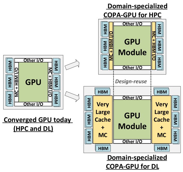
Nvidia’s latest stab at MCM GPUs is called the Composable On Package GPU, or COPA for short, and we will never use that abbreviation again beyond this story unless something, perhaps NVSwitch 3.0, is called CABANA. And this research is not really one packaging approach as much as it is a simulation of different packaging approaches for domain specific GPUs aimed at HPC and AI workloads distinctly. This is not the blueprint of future Nvidia datacenter GPUs so much as it is a discussion of the toolkit used to architect them and an affirmation that the HPC-AI convergence is going disharmonic at the socket level but that many components from within the socket will still be shared by future GPUs aimed at HPC and AI workloads.
The basic division that Nvidia is seeing is between HPC workloads, which need lots of FP64 and FP32 math capability and modest memory and memory bandwidth, and AI workloads, which need lots of lower precision math as well as some high precision floating point, and more importantly, a lot more memory capacity and memory bandwidth than the HPC workloads. (We find this hard to believe, as many HPC centers probably will.) The simulation work that Nvidia has done with its hypothetical GPU-N device is not changing the type and number of compute elements in the device – although that certainly could happen with the real GPU engines that Nvidia puts out this year and out into the future – but rather changes the way the packages implement cache and main memory for those compute engines using a chiplet design. Here are the basic feeds and speeds of the GPU-N simulation compared to Nvidia’s prior three generations of GPUs and a variety of machine learning ASICs:
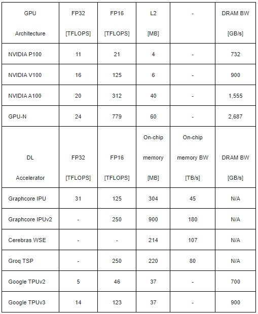
We presume that the GPU-N is implemented in a 5 nanometer process and represents a shrink of the existing GA100 GPU motor. (It does not say that anywhere in the paper, and this is a reasonable guess.) Assuming the ratios are the same, this GPU-N would have a mere 12 teraflops of FP64 performance – a lot less than the 45 teraflops that Intel is projecting for the Ponte Vecchio GPU and the 47.9 teraflops AMD is delivering for the Aldebaran GPU with their respective vector engines. Not that this paper shows this, but four of these GPU-N devices make 48 teraflops of FP64, and now the game is afoot across all three vendors. We are not saying Hopper or Lovelace or any of the other future Nvidia GPUs do this, but Nvidia has shown it can do it.
In any event, as configured for AI workloads, the GPU-N device has 60 MB of L2 cache on it, can crank out a very respectable 779 teraflops at FP16 and has HBM bandwidth weighing in at 2.7 TB/sec. Seems very respectable for an AI engine and an HPC engine, right?
Not so fast. Nvidia says that according to its simulations on GPU-N, having not enough memory bandwidth is contributing to the execution time of AI training and inference workloads, and that any increases in bandwidth based on a series of HPC benchmark tests “will go largely underutilized” on a converged GPU device that targets both HPC and AI workloads at the same time, like the Nvidia GP100, GV100, and GA100 GPUs do. If you cut the bandwidth on the GPU-N device by 25 percent, the HPC jobs only slowed down 4 percent and if you cut it in half – lower than what the A100 accelerator is delivering at 1.55 TB/sec – the HPC applications only slow down by 14 percent.
Hmmm.
To increase the bandwidth utilization on the HBM memory and to take some of the pressure off of it, Nvidia simulated the effect of adding larger L2 caches, and somewhere around 1 GB to 2 GB of cache is optimal for AI workloads. The only problem is you can’t put that much L2 cache on a GPU chip. So what is a GPU vendor to do? Add memory controller and L3 cache chiplets to the GPU package and mix and match capacities as the HPC and AI workloads dictate. Like this:
There are a lot of different ways of creating the GPU chiplet components by disaggregating the functions that might otherwise be on a giant, monolithic chip and then gluing them back together, and the GPU-N simulations took a number of disaggregation approaches, as shown below:
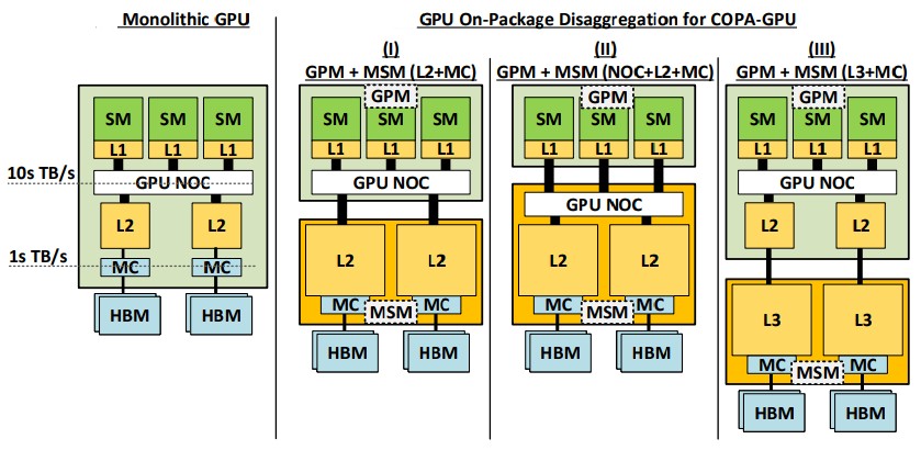
This architecture has a custom Memory System Module, or MSM, for a specific workload, be it HPC or AI, and very likely there could be variants for AI training and AI inference, depending on the need. The monolithic GPU like the P100, V100, and A100 are shown at the left of the image above. In one approach, the network on chip that connects the streaming multiprocessors (SMs) together remains on the compute chiplet and some fast I/O pipes come off the GPU NOC to link to a chiplet that contains the L2 caches and the memory controllers that link out to the HBM memory. In the middle approach, the GPU NOC is moved over the cache and memory controller chiplet and the L1 caches on the SMs link directly out to the external GPU NOC. And in the third option, the GPU NOC and L2 caches are left on the compute chiplet and the L2 caches link out to external L3 caches and memory controllers in the MSM, which in turn link to the HBM memory. Nvidia considered the options and went with option three on the right for the GPU-N simulation, mainly because it would take many tens of TB/sec of bandwidth to connect the GPUs to the NOC, and that would require a lot of energy.
Now that we have figured out the way to disaggregate the components, we have to figure out a way to stitch them back together, and there are a number of 2.5D and 3D options, which Nvidia outlined thus:
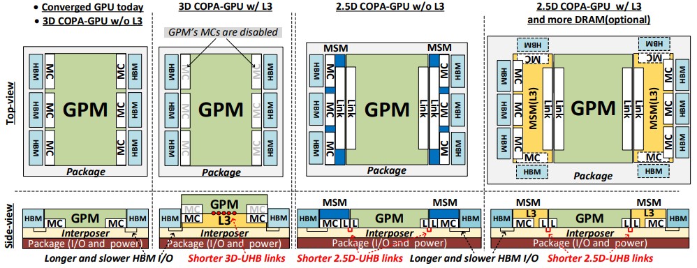
Again, on the left is how the Nvidia GPU engines are constructed today, with the memory controllers on the GPU die and both the GPU I/O and power and the memory controllers linking to the HBM through an interposer. The first option Nvidia simulated with the GPU-N device was to have an L3 cache placed between the GPU and the interposer and to put the HBM memory controllers on the same chiplet with short, 3D ultra-high bandwidth links between the GPU chiplet and the L3 cache and memory controllers on the MSM. The edge of the die with 3D packaging is limiting to the amount of HBM memory you can configure to the chip.
With the middle packaging option, a pair of MSMs sit beside the GPU compute, left and right, and are linked on the interposer through a quad of links to the L3 cache and to the memory controllers on the MSM, which in tern link to the HBM memory. This is in essence the future HPC GPU motor. With the third option, the MSM is loaded up with an L3 cache and 2.5D packaging is used to link the components together. This will be, we think, what a future Nvidia AI GPU motor looks like. Both in concept, of course. The point is, with separate MSMs you can put fast pipes between the GPU cores and the MSMs to keep them fed with data but also increase the edge length to add more HBM memory, as is shown in option three. For the third option on the right, Nvidia says it can do ten HBM sites on its MSM, and with a fatter one it could do up to fourteen HBM sites. That’s a lot more memory capacity and bandwidth. How much depends on the capacity and speed of the HBM, but it could be on the order of 2X to 3X what we see on the A100 accelerator – maybe higher – for the AI editions of future GPUs. The GPU-N simulation had 100 GB, which is not that impressive considering the revamped A100 has 80 GB already. Nvidia simulated a GPU-N with 1.9 GB of L3 cache and 167 GB of HBM memory with 4.5 TB/sec of aggregate bandwidth as well as one with 233 GB of HBM memory and 6.3 TB/sec of bandwidth. The optimal design running a suite of MLPerf training and inference tests was the for a 960 MB L3 cache and the 167 GB HBM memory with 4.5 TB/sec of bandwidth. By adding that L3 cache and boosting the speed and capacity of the HBM memory, the utilization of the compute engines rose and a single memory-enhanced GPU-N device was less costly than two plain vanilla GPU-N devices – and could do the same amount of work.
One interesting tidbit from the GPU-N simulations. Delivering 14.7 TB/sec of bandwidth over the UHB links in the 3D packaging scenario takes less than 4 percent of silicon and burns less than 2 watts; the 2.5D UHB link takes 6 percent of silicon and burns 9 watts.
All of this research strongly suggests what AI-optimized future GPUs from Nvidia will look like. The HPC variants, which need to deliver the best price/performance, will have one, two, and maybe four GPU chiplets and MSMs linking to HBM memory, and the AI variants will have one, two, and maybe four GPU chiplets with MSMs having lots of L3 cache and lots more HBM memory and bandwidth. And there is an outside possibility that there will be two future GPU chiplets – one with lots of FP64 and FP32 vector compute aimed at HPC and one with lots of Tensor Core matrix compute aimed at AI.
We are not entirely happy with this answer, should it all come to pass. With the HPC and AI hardware diverging, what happens when the workload uses a mix of HPC and AI software? Now we are back to buying multiple types of compute engines and locking in the ratios between them after having to make educated guesses on workloads many years in advance. The point of the GA100 GPU is that it is a general purpose device, that it can do anything and everything from virtual desktops to AI inference to HPC simulation to AI training to data analytics acceleration to visualization.
But this is what happens when Moore’s Law slows. You have to co-design everything. Hardware people have to know and listen to software people. There is no other way. Everything becomes a lower volume part and therefore gets more expensive, but each device does a very precise thing a lot better, so the price/performance keeps improving.

Datacenter Can Carry Nvidia Through The Rough Spots
After a decade and a half of ceaseless and focused work, Nvidia has created a modern compute platform, and a unique one at that. And while the collapse of the PC market and the Dot Coin Bust has not done its financials any favors in recent quarters, Nvidia’s datacenter business …
How Are GPUs Going To Change Your Working World? It’s AI, Everywhere
SPONSORED Mention GPUs these days, and you will naturally think about how they can accelerate the most challenging AI and machine learning workloads as well as how they are used in gaming platforms. But that’s only part of the story. The same platforms that underpin advances in both extreme AI …
Broadcom Takes On InfiniBand With Jericho3-AI Switch Chips
Variety is not only the spice of life, it is also the way to drive innovation and to mitigate risk. Which is why we are seeing switch architectures evolving to drive specific kinds of AI workloads, just as we saw happen with HPC simulation and modeling workloads over the past …
Too cute. The acronym for a three word phrase would have three letters. COP, not COPA. What does the ‘A’ stand for? What word does it expand to? Please, you are good at reporting tech and the market, and I know you can be very very good at proper grammar and sentence structure. Stick to what you are good at.
That was their term, not mine. I would suggest that the A could be Architecture. There are other options, obviously.
The abstract of the article in question has PA for “PAckage”. Perhaps the bulk of this article was written in 2020 when “defund the police” was particularly topical. “COP-GPU” also doesn’t roll off the tongue well, especially for non-native English speakers. Speakers of many languages would say “COPA-GPU” regardless.