

For decades, Intel leaned heavily on its manufacturing prowess as a key advantage over its various competitors like AMD, which had its own chip foundry that it spun off in 2009 and which became Globalfoundries. Its network of fabs allowed Intel to maintain control of both the design and manufacturing of its chips and more easily keep everything in line with Moore’s Law, from the earliest ideas through the eventual launch of the processors.
But as we have noted over the past several years, that manufacturing armor has been dinged, giving a growing crowd of competitors and chip-making foundries new life in a processor market that has seen Intel’s reign shaken a bit. Rivals like AMD and Arm were able to get to the 7-nanometer process level before Intel and are eyeing 5 nanometer and foundries like Taiwan Semiconductor Manufacturing Corp are growing their advanced manufacturing capabilities. Consolidation – such as Nvidia’s $40 billion bid to buy Arm and AMD’s $35 billion proposal to acquire programmable logic maker Xilinx – could mean that Intel will have much larger competitors to contend with in the near future.
Meanwhile, delays the launch of some chips – most recently the upcoming “Sapphire Rapids” Xeon SP processor – further fueled questions about whether Intel had lost its manufacturing mojo and would soon have to consider leaning more heavily on foundries to get its processors manufactured and on the market.
It was this situation that led some industry observers to be surprised in March when CEO Pat Gelsinger – the longtime Intel executive who returned earlier this year to lead to the chip maker following almost a decade at VMware – instead doubled down on Intel’s manufacturing future with the announcement of IDM 2.0, an acceleration of its integrated device manufacturing model that includes spending $20 billion to build two new fabs in Arizona, making chip factories in the United States and Europe available to other vendors processors as part of an expansion and formalization of its own foundry business, and using other third-party foundries to build some Intel products, such as chipsets graphics and communications chips.
Intel’s manufacturing future more recently made news with reports that the company was in negotiations to buy Globalfoundries for $30 billion (Globalfoundries has denied the rumors). All this comes amid an ongoing worldwide semiconductor shortage and pressure from the Biden Administration to grow U.S. chip-making capabilities.
The chip maker intends to regain its position as the world’s top manufacturer. At its Intel Accelerated event July 26, Gelsinger and Ann Kelleher, general manager of technology development, are outlining a processing and packaging roadmap that they argue will bring Intel to process performance parity in 2024 with other leaders and clear leadership a year later. The idea is to leverage the technologies available now – such as the SuperFIN manufacturing process and Foveros 3D integrated circuit – and bring on newer innovations over the next three years to remain competitive now while aiming for the leadership position down the road.
![]()
“We hit competitiveness earlier than leadership, true parity,” Sanjay Natarajan, senior vice president and co-general manager of Intel’s Logic Technology Development unit, said in a press briefing. “If you slice and dice, then there’s elements of competitiveness in here in different ways for different segments. In the meantime, what we have is, first of all, the ability to offer sort of a holistic solution, a lot of capability enabled by the packaging technology, where we can mix and match the best of what we can put together with the best that’s out there and ultimately deliver a compelling product and a package along the way. It’s definitely not the case that it’s all going to be elsewhere. There are going to be elements of it that are already quite compelling and competitive today. In fact, if you look at our 10-nanometer SuperFin products, they are competitive. That’s not just my opinion, but what we read from the outside telling us that we are making competitive products even today. I think at the product level, you’re going to continue to see a competitive landscape right away. I’m talking about process technology leadership being there in 2025.”
This is going to be done through a number of new innovations and adoption of advanced technologies, helped along by a number node-number system to make it easier for users, analysts and journalists to track the upcoming steps, Natarajan said. Currently, the 10 nanometer SuperFin products are in high-volume production.
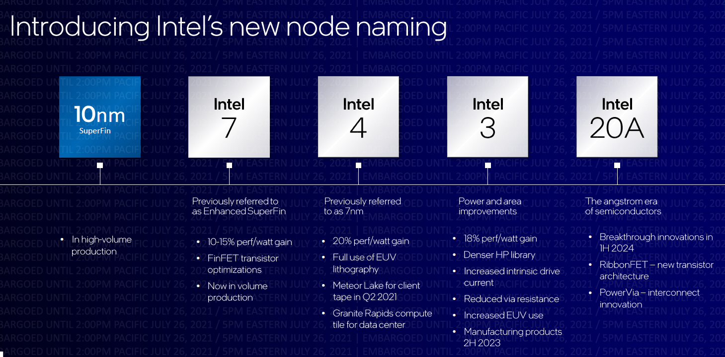
The new node naming also will mirror the reality of what’s happening in the industry, Kelleher said. It still is based on the idea that smaller is better, she said, but “I think the industry would agree with us basically that the measurement of nanometer really isn’t measuring anything on the transistor anymore. Based on that, we, along with the industry, have decided we needed to evolve our node naming. This is [the result of] a whole bunch of feedback we’ve gotten over the over the years in terms of our naming and as part of this we’re setting up basically a lexicon to talk about our process nodes and we’re setting up the framework so that it can be clear, consistent and meaningful. That allows our customers and the industry to look at our process nodes and make decisions on our process nodes and to make that much easier for everyone.”
Intel also will continue to stay focused on the performance-per-watt metric.
“One of the key aspects of, as you go from node to node, was the improvements in performance-per-watt that you get with each successive node and any success development,” Kelleher said. “That’s a key aspect of what we’re looking at in our process roadmap out as far as 2025.”
The company’s EnhancedSuperFin nodes will be referred to as Intel 7. They are still based on FinFET technology, which was first introduced at 22 nanometers, but it offers 10 percent to 15 percent performance-per-watt improvements over SuperFin. Intel 4 will be the new name for Intel’s 7 nanometer process, which will fully embrace EUV lithography to print the extremely small features by using ultra-short wavelength light. It will include not only area improvements but also another 20 percent jump in performance-per-watt. It will be ready in the second half of next year for products that will ship in 2023, including “Meteor Lake” chips for clients and “Granite Rapids” for the datacenter.
Intel 3 will be the last FinFET process and will begin to manufacture products in the second half of 2023, bringing about an 18 percent increase in performance-per-watt. It will include a high-performance library area scaling and Intel will increase the use of EUV, Natarajan said
The naming for Intel 20A is a nod to making the transition from nanometers to angstroms. The nodes will include a few key innovations, including PowerVia and RibbonFET. PowerVia is a backside power deliver system that switches the interconnects for delivering power and ground from the top of the transistor to the bottom. That will allow the power to be “delivered directly to the transistor without needing to go through the interconnect stack That virtually eliminates a voltage droop to the transistor. It’s a very big, significant savings in in power efficiency, and that does free up all of the wires on top for signal routing. It’s going to give us the opportunity either to do denser signal routing on the top or to do faster wires on the top and reduce the resistance and capacitance between lines.”
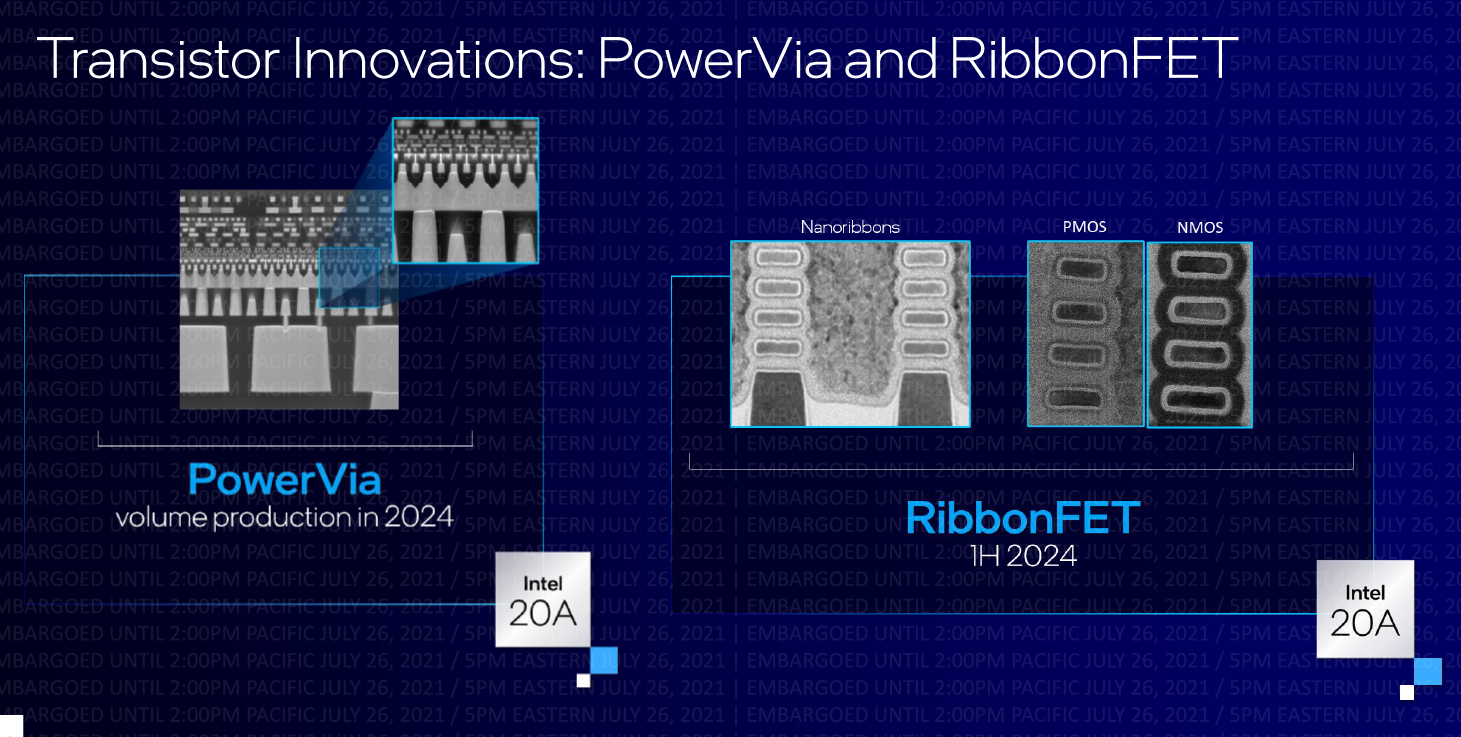
RibbonFET, which is Intel’s implementation of a gate-all-around transistor, will be the vendor’s first new transistor architecture since FinFET in 2011. It will come out with Intel 20A, which is expected to ramp in the first half of 2024 and will give Intel leadership parity in the industry. RibbonFET will feature multiple fins in a smaller area, delivering faster transistor switching speeds with the same drive current.
After 20A comes 18A, which is in early development and targeted for 2025. It will include more enhancements to RibbonFET that will drive greater transistor performance. Intel also is working on the next-generation High Numerical Aperture (NA) EUV, the next step in EUV. Intel is working with ASML on the development of High NA EUV.
Packaging also will be key. Intel has been using EMIB (embedded multi-die interconnect bridge) in products since 2017, thought Sapphire Rapids will be the first Xeon chip to ship in volume with EMIB. After Sapphire Rapids, the next EMIB generation will move from a 55-micron bump pitch to 45 microns. Meanwhile, Meteor Lake will be mark the second-generation use of Foveros – a wafer-level packaging technology introduced in 2019 with Intel’s “Lakefield” hybrid CPUs – in a client product. It will include a bump pitch of 36 microns, tile spanning multiple technology nodes and a thermal design range from 5 watts to 125 watts.
In 2023, Intel will roll out Foveros Omni and Foveros Direct. Foveros Omni will offer wide flexibility through a 3D stacking technology that will drive a die-to-die interconnect and modular design. It also will allow for the ability to mix multiple top die tiles and base tiles, giving Intel “a tremendous ability to mix and match our different styles together and build products that people were not able to look at previously,” said Babak Sabi, corporate vice president and general manager of assembly and test development at Intel.
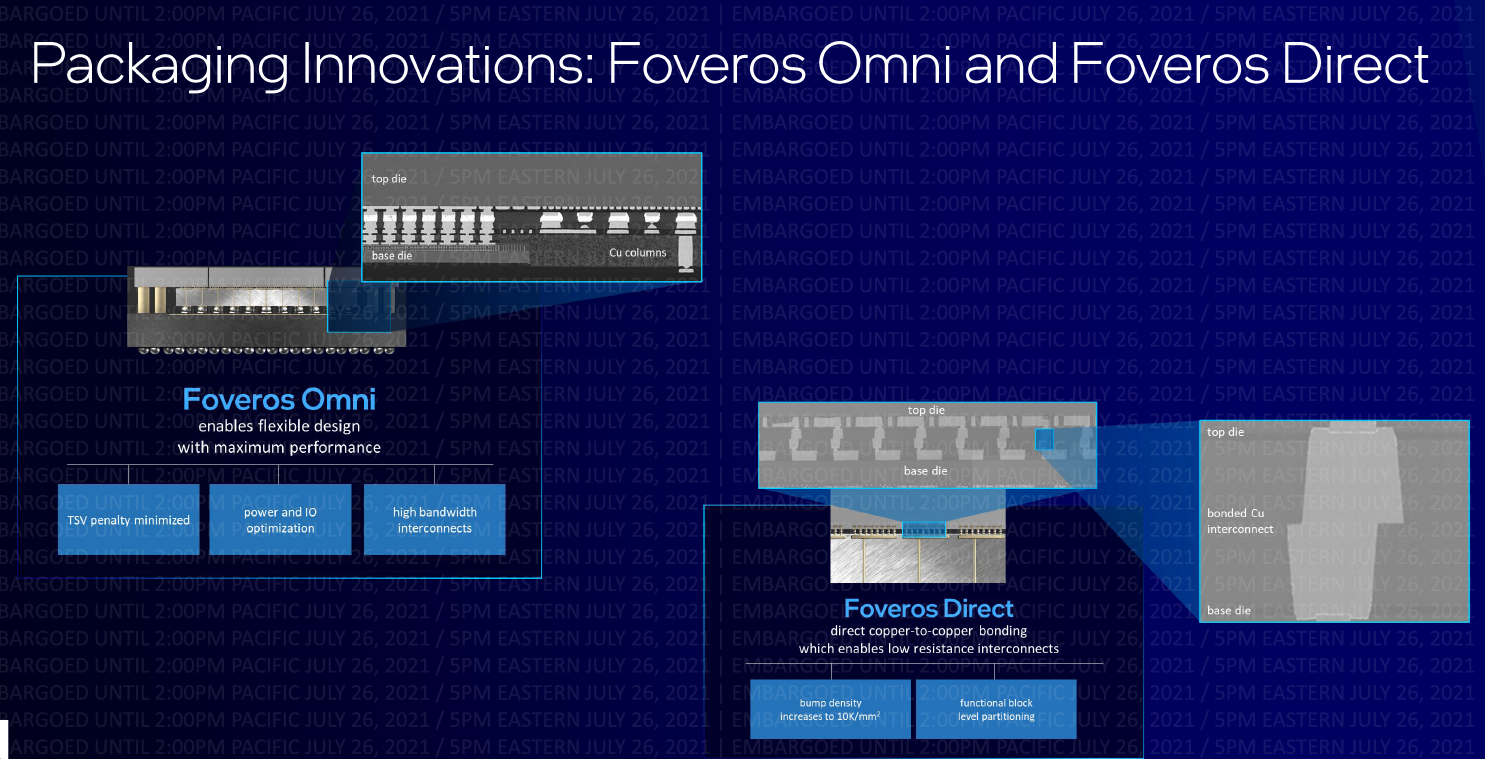
Foveros Direct, which will be complementary to Foveros Omni, will deliver low-resistance interconnects with direct copper-to-copper bonding. It also blurs the line between where the wafer ends and the package begins and enables sub-10 micron bump pitches, which will increase the interconnect density for 3D stacking. This will lead to new developments in functional die partitioning.


The press in general are unqualified scientifically illiterate morons that really only care about comparing a single digit dimensionless marketing number. This is as good a solution as any to addressing TSMCs “nanometer marchitecture dominance”.
Intels 10ESF process is as near as makes no difference identical in performance to TSMCs 6nm node.
We are not the press in general, however.
And you just did what you accuse people of. And when I comment, my name is on it. I don’t hide behind some fake billg@microsofa.com email. Which I have to admit is clever.