
The “Milan” Epyc 7003 processors, the third generation of AMD’s revitalized server CPUs, is now in the field, and we await the entry of the “Ice Lake” Xeon SPs from Intel for the next jousting match in the datacenter to begin.
The stakes are high for both companies, who are vying for what seems to be a reasonably elastic demand for compute capacity in aggregate around the world, even if there are eddies where demand slows and chutes where it accelerates. The room enough for Intel and AMD in the market, but it is the technical and economic jousting between these two that is going to make this fun and help spur future competition in the years to come.
We did our announcement day first pass on the Milan SKU stack, with the salient feeds and speeds, and slots and watts, the 19 new processors, and we also covered the actual launch event for the Milan chips by chief executive officer Lisa Su and her launch crew, which included Forrest Norrod, general manager of AMD’s Datacenter and Embedded Solutions Group, and Mark Papermaster, the company’s chief technical officer, and Dan McNamara, general manager of AMD’s server business.
Now it is time to get into the weeds for a little bit and talk about the Milan architecture and how this processor’s Zen 3 cores are delivering 19 percent higher instructions per clock than the “Rome” processor’s Zen 2 cores from August 2019. It is hard to squeeze more and more performance out of a core while maintaining compatibility, but Intel, AMD, IBM, and Arm Holdings are clever engineering companies and they often go back to the drawing board and rethink how the elements of a core are organized and pipelined. They always seem to find new ways to do things better, and it really is a testament to human engineering that this is true.
Someday, we presume, AI will be used to create blocks of logic and data from transistors and place them in a 2D or 3D chip layout and do a better job than people and their EDA tools; we talked about Google’s research in this area last year, in fact, and IP block placement in an EDA tool makes the games of Chess and Go look like a joke. So far, people are a necessary part of the process of designing a processor, so today is not that day. Ironically, better compute engines will hasten that day, and perhaps chip designers should not be so eager for such big improvements. . . . But, if history shows anything, you can’t stop progress because people just plain have faith in it. For better or worse. Often both. And we here at The Next Platform are no different in this regard, so don’t think we are taking some high brow view. Consider us raised eyebrows with the occasional furrowed brows. We admire what engineers do; we worry about what people do with what they create sometimes.
Mike Clark, an AMD Fellow who cut his teeth on the single-core K5 processors, the first in-house designed AMD X86 chip from back in March 1996, and the lead architect on the Zen 3 cores, walked us through the nitty gritty detail of the Zen 3 core that is at the heart of the Milan system on chip complex. Let’s dive in.
Right off the bat, this is a whole new, ground up redesign of the core – similar to what Intel is doing with Ice Lake Xeon SPs and their “Sunny Cove” cores and what IBM will be doing with the Power10 processor and its brand new core later this year. And the reason is simple: Everyone needs to push the IPC as hard as possible to boost single threaded performance, and then make tradeoffs in the SKUs between high clock speeds across a small number of cores and lower clock speeds against a larger number of cores to hit performance targets that are better on each class of workloads – and those in between – than their respective “Rome” Epyc 7002, “Cascade Lake” Xeon SP, and Power9 predecessors. You can’t just have more cores with a new generation, and you need to show better thermal efficiency at different performance points, too.
So how did AMD get that 19 percent better IPC with the Zen 3 cores used in the Milan server chips? By doing a whole lot of things all at the same time, as you will see. And when you contrast this with the lack of IPC improvements as the Sunny Cove cores are coming years late to market because of Intel’s delays with its 10 nanometer processes, it really shows:
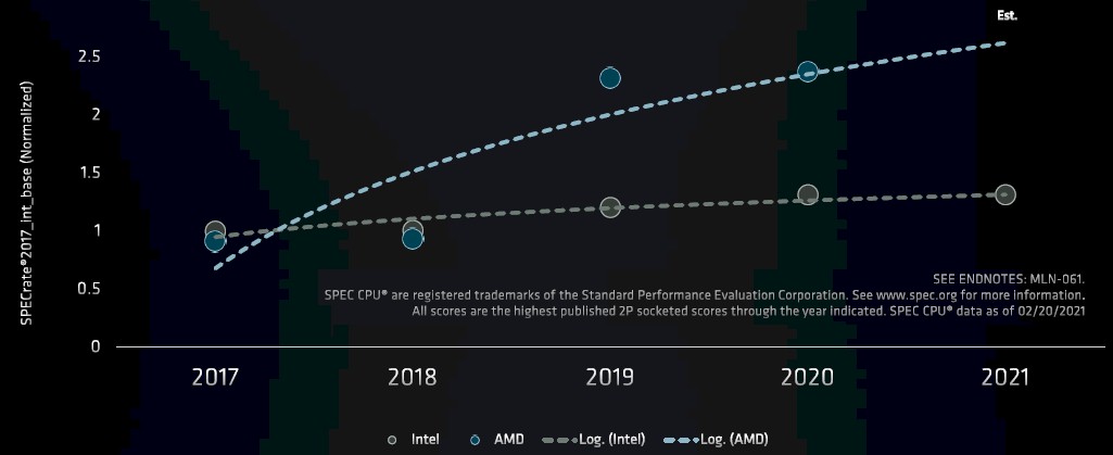
Intel was estimating Sunny Cove IPC improvements at around 18 percent last summer at Hot Chips and Zen 3 is offering 19 percent higher IPC in Milan. Their positions don’t change, hence the flat relative lines above.
“Here are some of the top-level performance improvements,” says Clark. “We improved branch prediction, and not just accuracy, but actually being able to get the correct target address out sooner and the correct target instructions out sooner and feeding them to the machine so we get more throughput, more performance. We have beefed up the width of integer throughput. We have doubled the intake floating point for inference, as we see those workloads evolving going forward and we are reacting to that. And by pulling the eight Zen 3 cores under the larger 32 MB L3 complex, we have better communication paths and we have more cache available for in lighter-threaded workloads and therefore we can reduce the effective latency to memory and provide more performance.”
The Zen 3 core still has two-way simultaneous multithreading, as we pointed out in our initial coverage, and AMD has resisted the temptation to add more threads to goose performance as IBM does with its Power architecture, which can dynamically switch from 2, 4, or 8 threads per core. (Sometimes, the threading in the Power9 and Power10 chips is set in firmware and the cores are fat or skinny, depending.)
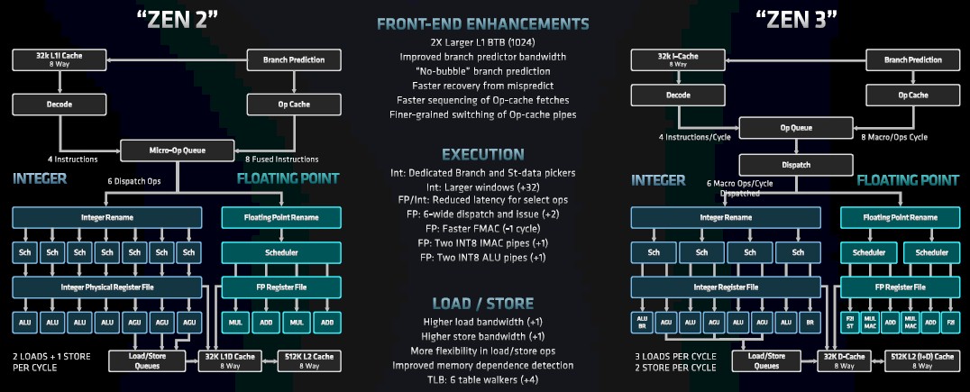
If you look on the right in the chart above at the Zen 3 block diagram, you can see there are two ways into the machine. The 32 KB instruction cache is still driven by a decoder that can drive four instructions per clock cycle into the op queue. And the way into the chip is through the branch predictor on the far right that can put instructions into the op cache and deliver eight macro ops per cycle. The dispatcher decouples the two sides of the Zen 3 pipeline – integer and floating point – and can do six macro ops per cycle to either unit.
That front end to the integer and floating point units in the Zen 3 core has a lot of tweaks, starting with a n L1 cache branch target buffer that is twice the size of the one in the Zen 2 core, at 1,024 entries.
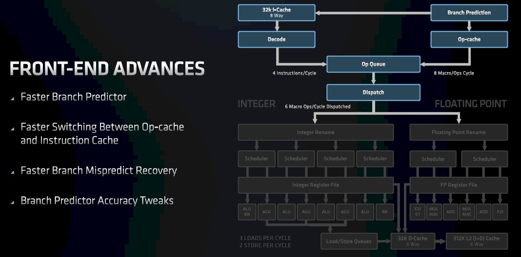
Clark says that the branch predictor on the front end has more bandwidth, which means it can pull more branches out per clock cycle. The Zen 3 core also features what Clark calls a “no bubble” branch prediction mechanism, which he explains thus:
“When you pull out a target address from the branch predictor, you then need to obviously put that back into the branch predictor to get the next address. Typically, that turnaround time creates a bubble. We have a unique mechanism where we can eliminate that bubble cycle and therefore be able to continuously pull out branch targets every cycle. We do still get some branches wrong in the execution units, but getting those addresses back and getting the target instructions of the machine – we improve the latency of that from Zen 2.”
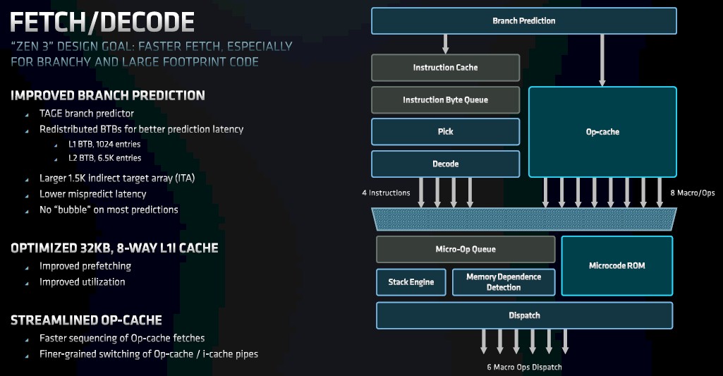
There are also some efficiency improvements in the op caches – faster sequencing of fetches and finer-grained switching of op cache pipelines – that help that Zen 3 front end drive that 19 percent IPC improvement (which is an average across a bunch of different workloads that have been used to gauge IPC on cores in the Opteron days that is now used on Zen cores in the Epyc era).
So that’s the front end – the air intake manifold and fuel lines in a car engine analogy, we supposed. What about the integer and floating point cylinders? Here is a zoom into the execution engine in the Zen 3 core:
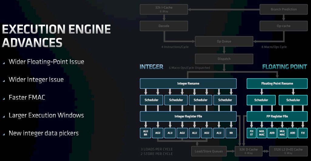
With the Zen 3 core, there is a much wider integer unit now, with four ALUs and dedicated branch and storage units, as you can see from the chart above comparing and contrasting with the Zen 2 block diagram in the chart further up in this story.
Here is a drill down into the integer execution unit, which Clark says has a design goal of having larger structures to extract more instruction level parallelism (ILP) from applications to feed this part of the execution engine; its units, in general, have lower latency, too. The combined effect is more integer IPC.
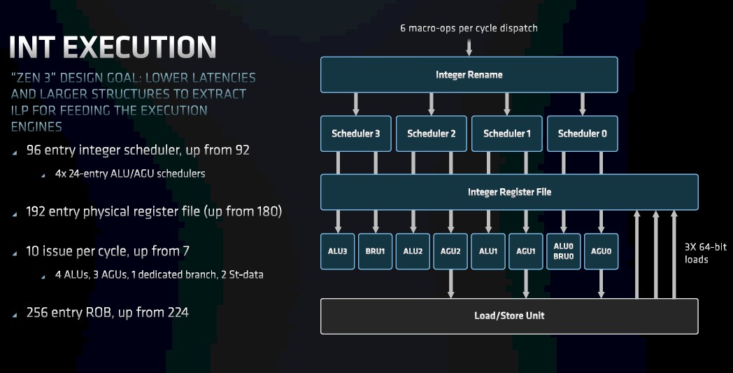
As you can see, everything increases by a little bit or a lot, bringing a different set of throughout and balance to the combined set of units.
(We wonder if the engineers play a kind of video game, tweaking this or that in a simulator so see the effects, or if the EDA tools do this work, as well. We suspect the former and that like much design there is a knack for it and as an architecture hardens a bit, you throw it out and start over. This Zen 3 core does not look that different from a Zen 2 core to our eyes – certainly not like the jump from Sledgehammer to Bulldozer to Piledriver to Steamroller cores.)
With Zen 3, there are four integer scheduler units instead of seven with Zen 2 (why seven, which so not base 2 and therefore violates our sensibilities?), and the same eight ports come out of the integer register file as with the Zen 2 integer unit. Rather than the schedulers being paired to an arithmetic logic unit (ALU) or an address generation unit (AGU), they are shared, allowing for balanced use across workloads. There are still four ALUs on the integer block, as you can see, but one of them has its own branch unit embedded in it and another one has a store unit embedded in it. Similarly, there are still three AGUs, but one has a store unit embedded in it. And, there is a branch unit pulled out separately.
“It’s still the same number of ALUs, but they are much more available and have much higher utilization,” says Clark. “With queue combinations, with shared ALU/AGU schedulers, which we can pick from independently, the pickers can get a better view of more operations to therefore find more instruction level parallelism in the workloads. And by offloading those extra store data and branches, those things don’t really return things back to the register file so you don’t really have to take the cost of having more write ports into the register file – just more read ports.”
With the Zen 3 core, the floating point unit is also wider, with six pipelines to be able to accept the input from that six-wide dispatch unit.
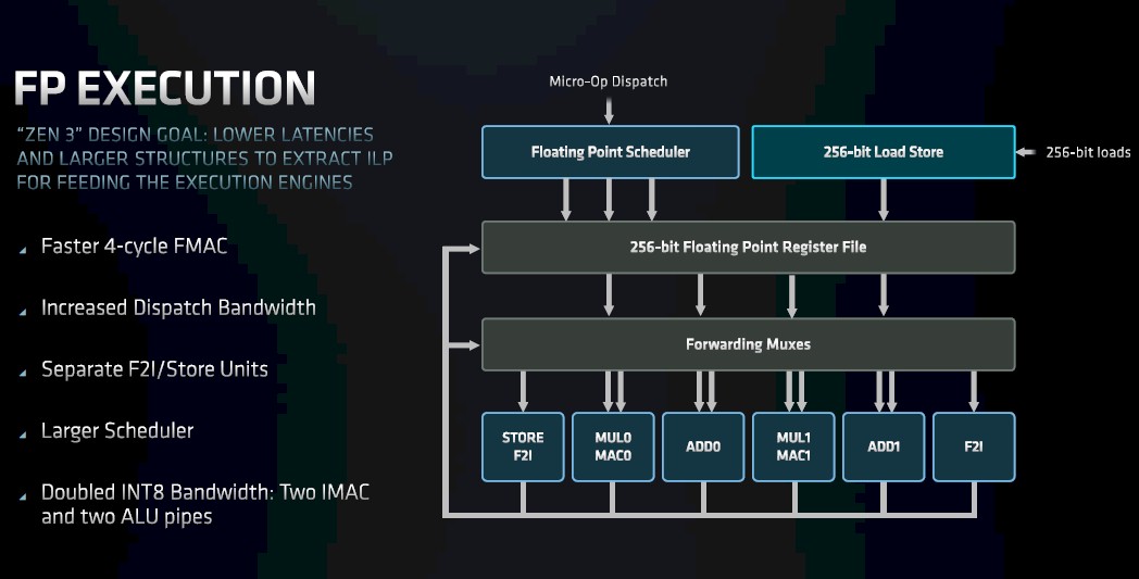
The floating point multiply/accumulate and add units have store units pulled out separately now, too. The reorder buffer has been increased in size so the Zen 3 core has a larger window to get more floating point instructions in flight. And, as with the integer units, the floating point to integer conversion units and store units are separated out from the add and multiple/accumulate units so they don’t collide or cause backups while still preserving the number of add and multiple/accumulate units compared to Zen 2. The floating point register file is 256 bits wide (same as with the Zen 2, which had a pair of 128-bit registers), and importantly for AI inference workloads, the INT8 bandwidth is twice that of the Zen 2 core, with two IMACs and two ALU pipes. The Zen 3 core can do two 256-bit multiply accumulate operations per cycle.
If you are going to chew on more data and instructions, you have to be able to load and store more data and instructions, so the load/store units in the Zen 3 core have also been beefed up:
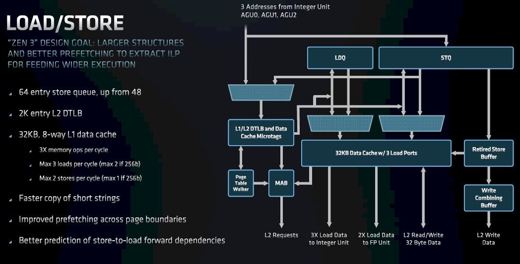
The Zen 3 core can do three loads per cycle or two stores per cycle, compared to two loads and one store per cycle (tied together, that is an and statement, not an or statement for the Zen 2 core). The load/store units have higher bandwidth per clock and, like the integer and floating point units, have greater flexibility in what they can do at any given time. Which drives up the ILP to get to that higher IPC.
Importantly, the Zen 3 core has six translation lookaside buffer (TLB) walkers, which walk that memory cache, which stores virtual memory addresses for physical memory in the DDR4 DRAM attached to each processor. This increased TLB capability, says Clarke, helps deal with server workloads that have a lot of random accesses to main memory or that have applications that have large memory footprints that span multiple pages of main memory.
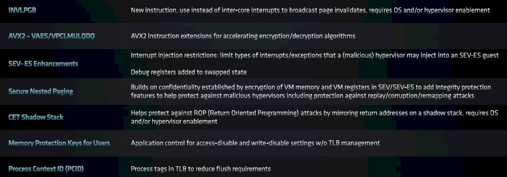
And finally, the Zen 3 core has a bunch of instructions that are added, as follows:
Next up, we will be taking a look at the competitive landscape as AMD sees it for the Milan Epyc 7003 processors.

AMD Gets Inside Facebook’s Latest – And Most Powerful – Microserver
Sometimes, you do put new wine in old bottles. This is what it looks like Meta – well, really its Facebook social network group – is doing as it adds a microserver node based on a custom AMD “Milan” Epyc 7003 processor to its datacenter infrastructure. Facebook has been one …

AMD Girds For Compute War With Xilinx Deal
The rumors were right, and AMD president and chief executive officer Lisa Su is indeed printing out a tower of stock to acquire FPGA maker Xilinx for what amounts to about $35 billion and, as it turns out, she is relinquishing her position as president to Victor Peng, chief executive …

The Acute Role Reversal For AMD And Intel In Datacenter Compute
Everything looked normal. An audience of company executives and employees, journalists, and analysts staring at the brightly lit stage as the chief executive officer strode from one side to the other boasting of a chip’s performance and power efficiency, the advanced technologies that went into making it, and the marked …
Statement; Calculate next 5 year compute market central processor component demand;
“The stakes are high for both companies, who are vying for what seems to be a reasonably elastic demand for compute capacity in aggregate around the world … ”
Intel Xeon ‘single’ Cores Production;
v2 = 4,252,137,318
v3 = 6,014,816,966
v4 = 4,336,668,585
XSL/XCL = 3,876,000,000
Xeon v2, v3, v4 volumes begin at their introduction date and on channel supply assessment produced in unison supporting end customer by generation platform standard through October 2019.
The question to consider; what is the base application CPU requirement in annual unit volume?
Xeon v2/v3/v4 total cores represent a relatively equal distribution.
Analyst base is v3 + v4 @ 10,351,485,551 total cores classifying v2 displaced on v3/v4 upgrade. In reality secondary market for v2 has been brisk in relation v3/v4 resale.
XSL/XCL core volume is deleted from this estimate as into first year of an upgrade cycle and here begins analyst’s 5 year growth projection.
Normalized by core count, at 16 core current commercial sweet spot, total available market without compute (data) elastic growth is 10.351 billion cores / 16 = 646,967,847 total components.
Note, thought lagging, enterprise application utilization in the 8 to 12 core range can be discounted from this estimate?
At 20C = 517,574,278 components is anticipated the near term enterprise sweet spot
‘
At 24C = 431,311,898
At 32C = 323,483,923 virtual machine sweet spot
At 64C = 161,741,962 represents a realistic Intel Xeon annual volume in relation slack additive.
Average Xeon 2012 to date is 200 million annual decreasing by 1/2 through three years of XSL/XCL = 300 M units.
Ivy full run in units = 495,587,100
Haswell = 648,148,380
Broadwell = 368,138,250
XSL/XCL = 300,000,000
See the upgrade cycle? The question is elastic application demand and I’m not talking component variable core operation. Or am I?
At x2 data CPU relation the next 5 years commercial data center market for compute is the equivalent of 20,702,971,103 cores or 323,483,923 individual 32 core components.
Agree, disagree, define.
At 32C normalized / 5 = 129,393,569 components on production economic assessment is thought current Intel Xeon annual production across all core grades.
Scalable XSL/XCL full run by core grade;
4C = 8.08%
6C = 4.65%
8C = 23.40%
10C = 9.77%
12C = 15.17%
14C = 4.81%
16C = 9.86%
18C = 6.69%
20C = 5.03%
22C = 1.48%
24C = 4.14%
26C = 1.96%
28C = 4.97%
Rome full run by core grade;
8C = 14.51%
12C = 3.39%
16C = 15.67%
24C = 11.88%
32C = 31.92%
48C = 2.93%
64C = 19.71%
Query; at xx% component growth per year, analyst relied on 19%, reaching 259,477,998 central processing units in 2025, what is the annual by core grade requirement 2001 through 2025? On analyst standard distribution median is set at Rome 32 core.
Mike Bruzzone, Camp Marketing