

Every chipmaker has an emerging silicon photonics story but as happens only rarely, it could be a small startup that will push them to productize faster.
Lightmatter, with its “Passage” wafer-scale photonic interconnect, might be the key to letting large numbers of accelerators communicate quickly and efficiently, leading to far denser systems for workloads like AI training, in addition to providing a more dense and power efficient platform. The company has more than just an interconnect—the newly-released Envise AI accelerator chip bundles up the company’s work in photonics and silicon design with the software tools to back it up.
And what should certainly get the attention of the major early players in rolling out silicon photonics products is that all of Lightmatter’s work in the interconnect, traditional semiconductors, and AI software is being sampled as a full plug and play system.
If you were to glance at the 4U blade silicon photonics startup, Lightmatter, is letting some key early customers evaluate now, there would be nothing to set it apart—at least on first glance. But inside is one of the first commercial efforts from a small company to push compute density and power efficiency to AI market where it is most needed.
Each of the company’s new blades has 16 of its Envise photonic computing chips, which they are pushing as a general purpose machine learning accelerator, complete with the Idiom software stack with compiler toolchain, debugger, profiler, and other features to present that desired “plug and play” capability for models built in PyTorch or TensorFlow, among others.
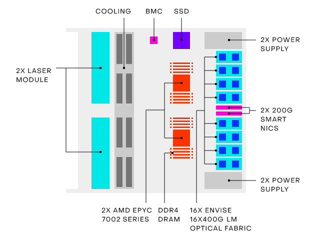
As shown, each of the blades has 3TB NVMe SSD with 2 AMD Epyc 7002 host processors. This choice was more about timing, Harris says, with Ice Lake delays pushing the decision.
As the company’s founder and CEO, Nick Harris, tells us, the real advantages are in compute density and power consumption. Each blade consumes 3kW (compared to an equivalent based on Nvidia’s A100 at 6.5kW). He also says that each of the Envise chips is faster than the A100 on a wide set of benchmarks, although we have yet to see more info on that based on MLperf or other metrics to date, only their own internals.
The Envise chip itself is not remarkable in terms of the core compute elements, it’s the pairing of photonics and traditional semiconductor technology into a single module that makes it interesting. The hardware supports common activations, convolution acceleration for common filter sizes, support for Int-8, Int-16, and bfloat16, and dynamic scaling for dialing precision.
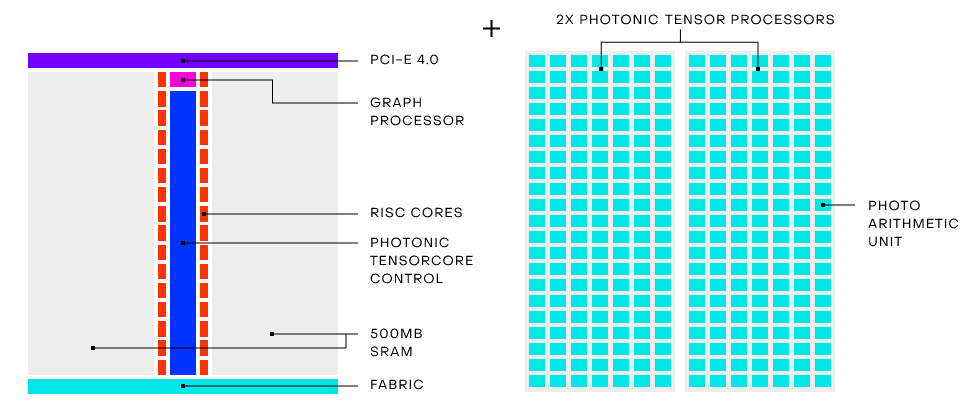
Each of the Envise chips has 500MB for sizable handling of on-chip activation and weights, offload is handled by 256 RISC cores per processor for general offload handling, and the 400Gbps Lightmatter interconnect fabric on each chip is designed for large-model scale-out.
They’ve worked in other features, including virtualization so multiple users can occupy the Envise chips and it has scale-out capabilities, including the ability to add a top of rack switch and ample optical I/O for the 2-chip Envise cards. “That’s 6.4 terabits/sec bandwidth so you can build very high speed meshes and other configs for high performance scale-out ML,” Harris explains.
“We can provide more compute per rack, not leaving any rack space empty and that’s really important because it saves area in dc and power and driving compute density. The other thing is just that our chips are faster, we really want to power the growth in AI–if you want to continue powering that you need a new compute technology and that’s what photonic compute is about. Delivering something that is faster, takes less energy so the environmental impact of scaling AI isn’t so detrimental,” Harris says.


A Five-Year Challenge Roadmap for Photonics-Based Computing
Silicon photonics has been proving its worth in telco and communications but there is a much brighter opportunity photonics-based computing. The energy efficiency and data movement potential is promising, especially for increasingly data-laden analytics and AI/ML applications, but the road to a diverse hardware ecosystem for compute is still long. …
How Lightmatter Breaks Bandwidth Bottlenecks With Silicon Photonics
Without question, the biggest bottleneck in artificial intelligence and for a lot of HPC workloads today is bandwidth. Bandwidth at the network level; bandwidth at the socket level; bandwidth at the compute and memory level. No matter how many teraflops one single chip can push at high precision, once your …
Imagine an AGI running on a photonic chip, “consciousness” emerging from simple photons! Crazy…
Imagine an AGI running on a photonic chip, “awareness” emerging from simple photons! craziness…