

For the past several years here at The Next Platform, as we have been pondering what IBM might do with the future Power10 processor, we have been feinting here and there with our analytical pen, trying to suss out precisely what Big Blue might be up to, particularly with the unique memory architecture that it has been working on for more than a decade.
Now we know. Power10 is not just a very elegantly designed chip, but a cluster of systems linked tightly – as tight as tight can be when it comes to systems – by their main memories. This architecture has been evolving since the company was involved in the supercomputing architecture explorations of the US Defense Advanced Projects Research Agency that resulted in the creation of two supercomputer variants of the Power7 processor back in 2010. Both machines were the result of the PERCS project that IBM was awarded by DARPA in November 2006, which gave IBM $244 million to develop future hardware and software. With Power10, IBM is extending and commercializing the technology foundation laid out by the PERCS project so many years ago.
We can’t tackle this new architecture and do it justice all in one fell swoop. So we will do it in two pieces, talking about the Power10 processor first and then this new memory architecture second. And as an added bonus, we will try to answer this simple question: Just how in the hell did IBM lose the two exascale supercomputing deals at Oak Ridge National Laboratory and Lawrence Livermore National Laboratory? With what IBM is bringing to bear, this should have clinched the deal, and it might mean that future AMD Epyc processors will have similar SerDes-based memory and I/O controllers and hardware-based memory coupling with global addressing.
So, without any more fuss or muss, let’s drill down into the Power10 processor.
A Cloud By Any Other Name
To begin with, as far as we know, IBM did not give the Power10 chip a code-name, which is not only hard to believe even if it is true, it is silly particularly if it is true. Code-names give us variety in our language, which comes in pretty handy when you are communicating. Besides, cool names matter. We are human beings after all, and labels don’t just have meaning, they have magic. And thus, we are going to bestow a code-name on the Power10 chip, a baptism of sorts to honor the work that IBM’s engineers did and that the marketing people that might have squelched this sort of thing, for some reason, cannot understand.
The low-end Power9 chip was called “Nimbus” internally at IBM, and the high-end Power9 chip aimed at big NUMA iron was called “Cumulus,” both in keeping with the increasingly cloudy nature of server infrastructure these days. These are the big storm clouds, and they sometimes merge into cumulonimbus clouds, spanning from the ground level all the way up to 12 kilometers above the surface. For Power10, given its more ethereal nature, we formally dub it “Cirrus,” those wispy dragon and phoenix clouds that are up high in the sky, between 9 kilometers and 12 kilometers, the outer edge of the troposphere.
Now that we have that out of the way, let’s talk about IBM’s Cirrus processor, which is expected to come to market in systems a little more than a year from now.
The Power10 presentation at Hot Chips this week was given by William Starke and Brian Thompto. Starke is chief architect of the Power10 processor and has been involved in the designs of many generations of Power chips from IBM. Starke talked to us about the focus that Power10 would have on bandwidth back in August 2019, and then we also had a conversation about the Power9’ “Axone” processor, a kicker to the Power9 chip that implemented a prototype of the Power10 memory subsystem, that was supposed to have been announced last year but has not seen the light of day. (Our guess is that this prototype was aimed at giving the HPC centers buying exascale-class machines a software development platform had IBM won the contracts at the US Department of Energy.) Thompto is the Power10 core architect, and specifically was in charge of a ground up recasting of the Cirrus core, with a focus on improving energy efficiency in every aspect of the core.
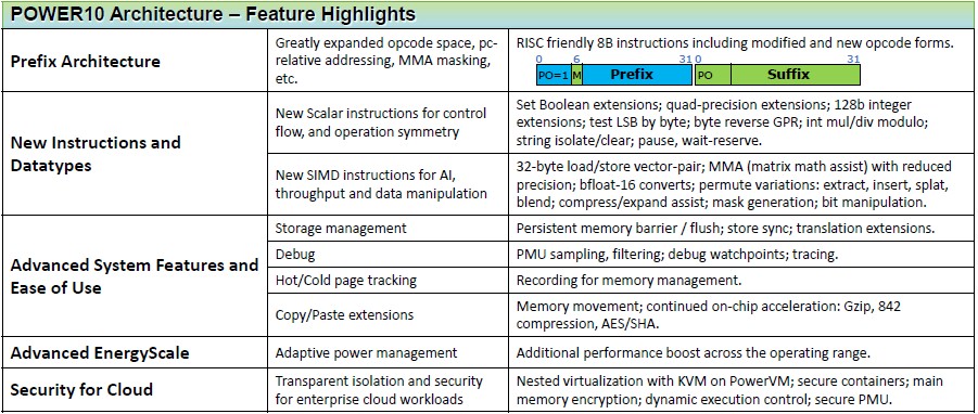
The Power10 core adheres to the new Power instruction set version 3.1, which was open sourced under the OpenPower Foundation last August. The Power10 core has over 200 new instructions that have been added, according to Thompto, and these are aimed at making the microarchitecture more efficient at certain functions as well as adding new functions. Here is a breakdown of the important new instructions and data formats supported in the Power10 core:
The important thing for commercial and HPC workloads alike is that the Power10 chip supports the mixed precision floating point and integer formats in its vector and matrix math units that allows it to support machine learning training and inference workloads natively on the processor. We doubt very much that machine learning training will be done very much on Power10 chips, but we certainly do believe that inference is going to happen on the host processors, not on accelerators, because it will need to be embedded in applications and done very closely with the other processing in the application. If inference is going to be a relatively light and sparse part of a commercial application, this only makes sense.
Here are the feeds and speeds of the SIMD vector engines and matrix math assist (MMA) units on the Power10 chip, which shows the path from the OpenCAPI Memory Interface (OMI) on the DDR4 memory buffer that the Power10 memory sticks uses all the way back to the matrix math unit.
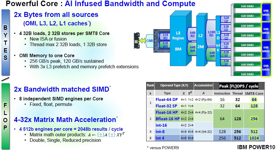
The data shown above is for the fat Power10 core that has simultaneous threading set up with eight threads per core (known as SMT8 mode within IBM). For Power10 chips that IBM locks into SMT4 mode, cut the number of SIMD and MMA units in half per core and then multiply the total number of cores on the die by two. It comes to the same, it is just about tweaking the hardware for performance and for per-core software licensing.
As you can see, the vector units support the standard 32-bit single precision and 64-bit double precision floating point that is the mainstay of HPC workloads and that is also often used by AI workloads. But the math units on Power10 also support two flavors of 16-bit half precision floating point – the IEEE float-16 format and Google’s better Bfloat-16 alternative, which has a greater dynamic range than FP16 and in fact is the same as FP32. Some precision is sacrificed without giving up the dynamic range for numbers, and for AI this is a tradeoff that has very little impact on machine learning training and inference results and allows for more data to be run through the math units in any given time, which has a huge impact on machine learning results. Intel’s “Cooper Lake” Xeon SP processors, announced in June, support Bfloat16 processing in their vector engines, and so do Nvidia’s “Ampere” A100 GPU accelerators. Obviously, Google’s TPU AI engines also support the Bfloat16 format, which it was invented for, and so will future Prodigy processors from Tachyum and the Neoverse Arm server chip designs from Arm Holdings. Both Ampere Computing and Marvell have slated Bfloat16 support for future Arm server chip designs.
The Power10 chip also supports 4-bit, 8-bit, and 16-bit integer operations, which are mostly important for machine learning inference workloads. The math units accumulate into 64-bits or 32-bits, depending, and provided twice the SIMD processing capacity of the Power9 chip and anywhere from 4X to 32X the matrix math capability. This is a significant speed bump for a processor, and there are plenty of customers who will be able to use Power10 chips for inference without the need for accelerators – much as they can do with Intel CPUs in the datacenter.
Let’s zoom in on the Power10 core and work our way down into the microarchitecture and then out to the system on chip. Take a gander at the core:
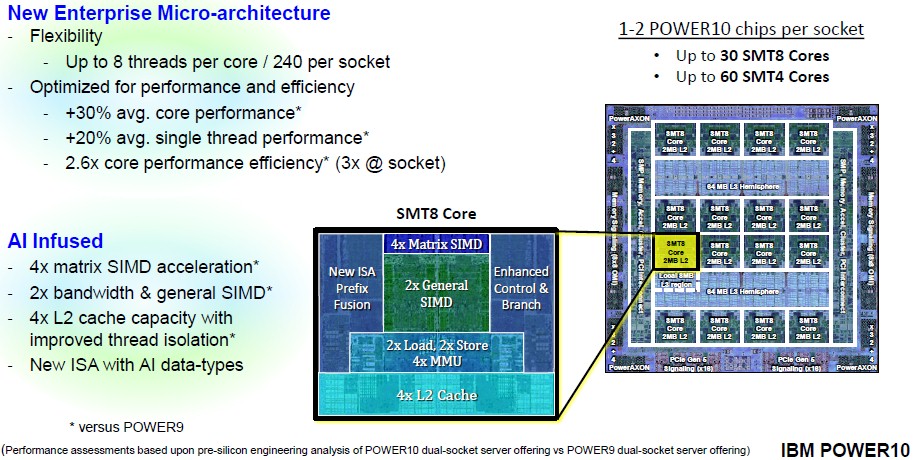
Again, this is the SMT8 version of the Power10 core, and you can see the 2 MB L2 cache segment on the core, which is four times as large as the L2 cache on the Power9 core. There are twice as many load and store units and four times as many memory management units, and these feed into those SIMD and matrix math units, which are 2X and 4X as big as on Power9, respectively. Based on pre-silicon simulation of a two-socket Power10 server, this setup yields about 20 percent better single thread performance over a two-socket Power9 server at a normalized 4 GHz clock cycle, and the average core performance is up by 30 percent (presumably including a smattering of math from those SIMD and MMA units).
Drilling down into the microarchitecture, here is how the flow through the Power10 core works:

This is only showing half of the SMT8 setup, which would be hard to draw and which is equivalent to the SMT4 core. You can see the four 128-bit execution slices at the heart of the system, which is front-ended by a 48 KB L1 instruction cache and backended by a 32 KB L1 data cache. A lot of the features of this Power10 core are 2X or 4X that of the Power9 core, as you can see, although some are only moderately improved. Add it all up, and the SMT8 core yields 30 percent more work on average and thanks to the design, the process shrink from 14 nanometer processes from GlobalFoundries used with Power9 to the 7 nanometer processes from Samsung (which have some extra IBM goodies baked in and are not just Samsung’s V1 process), the power consumption per core has been cut in half. That’s a factor of 2.6X improvement in performance per watt, which sounds like a lot between generations but you have to remember there will be almost four years between the Power9 and Power10 generations, too.
This is impressive improvement, but imagine if IBM could do this on a two-year cadence?
IBM is holding the wattages more or less constant for its sockets relative to the Nimbus and Cumulus sockets in its Power Systems machines, but is not divulging what those watts are. What Starke did say is that a Power10 socket, again normalized for 4 GHz performance, would have about 3.25X the integer performance and 3X the floating point or Java performance, and 2.25X the memory bandwidth performance of the Power9 socket.
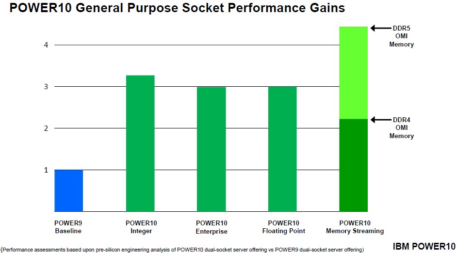
That memory bandwidth figure, which is base don the STREAM Triad benchmark, is interesting in that this is pitting direct attached DDR4 memory on the Power9 against the OMI memory with a buffer on the DDR4 memory stick and driven by the Serdes on the Power10 chip. The SerDes and buffer setup adds about 10 nanoseconds to memory accesses, so it is not free but it is nominal. But the interesting bit is that because that OMI SerDes is not hard coded for DDR4 – the buffer chip is – when DDR5 memory comes along, it will sit behind the same buffer and can be swapped right into a Power10 machine and suddenly the memory performance will double again without having to change the processor or the system.
Neat.
Having talked about the performance of that socket above, we should probably have a look at the socket. So here is the Power10 die, hardened into SMT8 mode, with its features labeled:
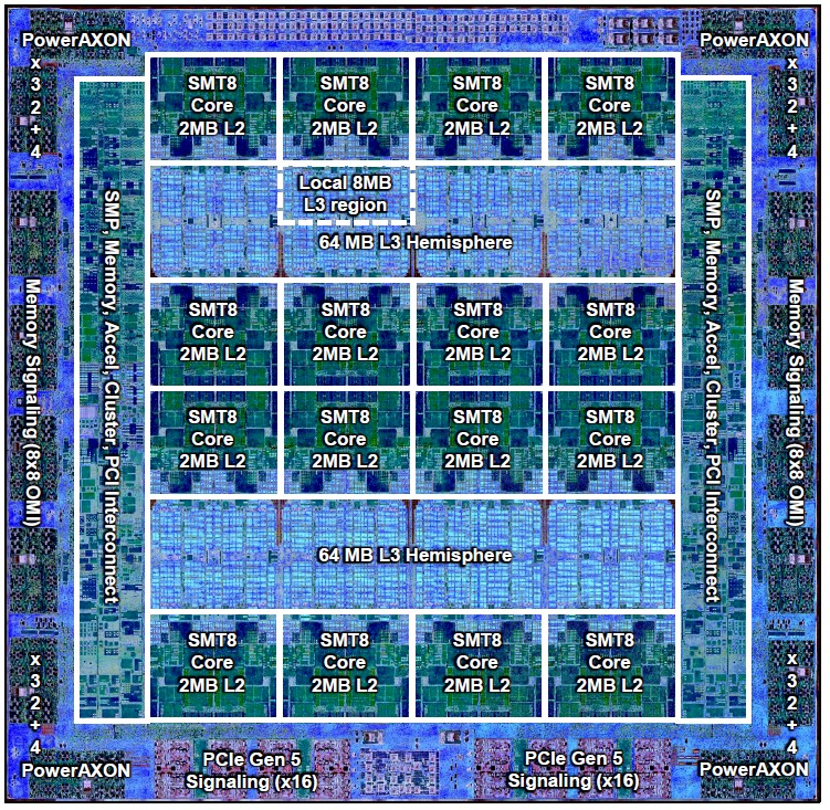
As you can see, there are 16 cores on the Power10 die, but IBM is only firing up 15 of them (or 30 if it is in SMT4 mode) for applications to use. That 16th core is not so much a spare as one that IBM is pretty sure statistically is going to be a dud given the yields on the 7 nanometer processes at Samsung, which is making its first server chip ever with IBM’s Power10. Power10 makes the Samsung Exynos processors used in client devices and smartphones look like a toy. And it is, by comparison. In any event, at some point, when yields improve, IBM will be able to sell that 16th core, and you can bet your last dollar it will do so.
The Power10 chip has 18 billion transistors, which is fairly light in the modern era, and it weighs in at 602 square millimeters in area with 18 layers of metal stacked up. The chip has 128 MB of L3 cache, and it is interesting that IBM is not using its embedded DRAM design as it has for Power7, Power8, and Power9 but rather regular SRAM etched by Samsung, which Starke says IBM can do thanks to the process shrink.
Here is the interesting bit. All of the roadmaps we saw behind the scenes over the years for Power10 pegged it at 48 cores. Now, we highly doubted that IBM would cram 48 cores on a monolithic die, even at 7 nanometers, because of the yield issue mentioned above, and we just figured IBM would basically shrink the Power9 chip, add the improved I/O and memory SerDes, and put two of them into a single socket in SMT4 mode to get to 48 cores. Maybe that was the plan, but this is not what IBM actually did.
Rather, IBM went all the way back to the drawing board and created a chip that had had 16 SMT8 cores or 32 SMT4 cores and it also went with a dual-chip module option to double up the number of cores with a modest decrease in clock speed on the cores and still keep within the thermal envelope it sets for its own Power Systems. So it can deliver either 30 fat or 60 skinny Power10 cores in a socket, with a total of 240 threads per socket.
To keep that beast fed, there are 16 x8 (eight lane) OMI memory interfaces with a total of 1 TB/sec of bandwidth (lanes run at 32 GT/sec), and there are also 16 PowerAXON x8 interfaces at also run at 32 GT/sec and deliver 1 TB/sec of bandwidth. These PowerAXON interfaces can run NUMA or OpenCAPI interfaces, and there is no good reason why they can’t run the NVLink 3.0 protocol used with the Nvidia A100 GPU accelerators, but the fact is that they don’t. (Hmmmm. . . . ) The Power10 processor also has two PCI-Express 5.0 controllers with 16 lanes each, which doesn’t sound like a lot until you realize IBM wants a lot of stuff to come into the Power10 chip over PowerAXON links. We will see if IBM supports Intel’s CXL protocol over those PCI-Express 5.0 controllers. There is no reason why this can’t work, and that IBM could not, in theory, support AMD Radeon Instinct and Intel Xe GPU accelerators over PCI-Express links. But, that would limit connectivity to two GPU devices per CPU, unless a PCI-Express switch was used. It is not clear if coherence would be provided here between CPU and GPU memory over the PCI-Express protocol, but there is no reason why it could not work – in theory – if IBM still wants to sell hybrid CPU-GPU systems. Which we presume it does.
Here is how IBM is initially thinking about implementing Power10 in servers:
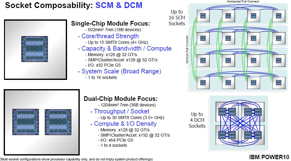
We think there will be variations on these themes, with SMT4 variants of Power10 also available as needed. But as you can see, IBM is going to be focusing its NUMA big iron on the single-chip module, scaling out to 16 sockets as it has done in Power8 and Power9 machines, but it is using Power10 dual-chip modules in machines with up to four sockets. To double up the cores per socket, IBM only has to slow clock speeds down by about 12.5 percent (from around 4 GHz to around 3.5 GHz) but still put 1.9X the performance in the box and still have a lot more I/O in the system and the same memory capacity in the system. This is a fair trade.
By the way, this is not IBM’s first rodeo with dual-chip modules. Systems with Power5+, Power6+, Power7+, and Power8 processors all had some variants with DCMs, whether customers knew it or not.

IBM Views Enterprise Storage Through Hybrid Cloud Glasses
For the past couple of decades, IBM’s Spectrum Scale – formerly known as General Parallel File System –has had a solid standing as one of the two go-to file systems for HPC. However, the emergence of modern workloads like artificial intelligence and analytics, coupled with the rapidly expanding growth of …
IBM Power10 Shreds Ice Lake Xeons For Transaction Processing
Here is a simple algebraic equation that describes the relative computing oomph of two different CPU architectures over the past two decades: If Intel an X86 core is X, then an IBM Power core equals 2X. IBM’s Power family of processors and their resulting hardware systems has never been particularly …

The Future IBM We Will Probably Never See
Let’s get one thing straight right off the bat. If someone has been named president of International Business Machines Corporation, it means they are the heir apparent and future chief executive officer of what used to be the world’s largest IT supplier. Which is why the announcement of the departure …
amazong chip! the new memkey sharing capability is going to be a game changer!
Good analysis! Power10 did have an internal code name, but you’d be forgiven for being confused by it. The code name is “Power Ten”, which is apparently a term used in rowing when the rowers go all out for ten strokes.
I’m looking at the official IBM press release in which it details the footnote on comparing Power10 to Power9 with the phrase “3X performance is based upon pre-silicon engineering analysis of Integer, Enterprise and Floating Point environments on a POWER10 dual socket server offering with 2×30-core modules vs POWER9 dual socket server offering with 2×12-core modules.” My reasoning says
30 cores/12 cores = 2.5
so most of the 3X speedup comes simply from increasing the core count. Seen another way, since
3.0/2.5 = 1.2
it would appear the per-core speedup is only 20 percent. While that would be fine for a one or two year release cycle, it’s been 4 years.
As the single-core performance of Power9 on processor-bound scientific workloads was less than half something like the Xeon Gold 6126 a year ago, it is completely unclear whether the announced 20 percent per-core performance gain of Power10 is much to boast about. I sincerely hope it is, because the IBM Power has many other advantages that would be short changed if the built-in floating-point arithmetic is slow.
In my opinion, the Fujitsu AFX64 used in the Fugaku supercomputer shows that combining high bandwidth with scalable vector instructions all in the CPU core leads to GPU-like levels of performance that is much easier to write code for. This is important, because research science depends on creating new programs to solve new problems using new algorithms.
wow their slides are so bad (== good for engineers), Nvidia is really good at hyping the smallest upgrades to their architecture, here similar upgrades are mentioned in a bloated text section.
They need to learn how to hype for the general public, sadly we engineers aren’t too good at that 🙂
@jimmy I think you may be right about the slides.
I had another look and it appears the 512bit vector engine does support double precision, which I didn’t see before. There is also another slide that mentions a 10x improvement over Power9 on Linpack.
The same calculation as before to correct for the differing number of cores
10/2.5 = 4
suggests a 400 percent per-core speedup. This is much more competitive.
While a petabyte of shared RAM sounds amazing, price performance at the entry level is crucial for business that want to grow and for independent developers to polish the open source software needed at all scales.
Hopefully the availability of the Power10 and the end of the epidemic will soon be two good news stories.