
The term “general purpose” in regards to compute is an evolving one. What looked like general purpose in the past looks like a limited ASIC by today’s standards, and this is as true for GPUs and FPGAs as it is for CPUs.
There is much talk about the era of general purpose computing being over, but we think that it is probably more accurate to say that the era of CPU-only computing – with the CPU being the only general purpose compute engine available for many decades – is over. If general purpose means being able to run lots of different kinds of applications and do lots of different kinds of compute, a fair argument could be made that over the past decade, GPUs and FPGAs have been just as “general” as CPUs. Perhaps moreso. And this would be true without question if Nvidia had gone through with “Project Denver” and embedded Arm cores onto its GPU motors, which was announced in early 2011 and canceled a few years later. And it certainly is true for the FPGAs from Intel and Xilinx, which have embedded Arm cores and which have more kinds of compute than you can shake two sticks at.
We have come a long way from the first generation of so-called “general purpose graphics processing units,” or GPGPUs, that Nvidia launched way back in 2006 with the “Tesla” G80 GPUs and evolved substantially in 2010 with the “Fermi” GF100 and GF104 GPUs, and really kicked it in with the “Kepler” GK104 and GK110 GPUs two years later. As workloads have been added to GPUs, they have gotten more general, expanding from raw floating point compute to accelerated HPC to accelerated AI training, ending up with a mix of integer, floating point, and matrix math capability in the end.
With the “Ampere” GA100 GPU, as we discussed at its launch and analyzed further in the deep architecture dive that followed it, Nvidia is essentially converging the jobs performed by its prior generation “Volta” GV100, used in the V100 accelerators, and “Turing” GT104 GPUs, used in the T4 accelerators as well as GeForce cards. Volta was the HPC simulation and AI training engine that was also useful for database acceleration and certain kinds of analytics workloads like the Spark in-memory platform. Turing was aimed at AI inference as well as graphics related to virtual desktop infrastructure (where the GPU is carved up into slices), to technical and artistic workstation applications and to gaming. With Ampere, the GA100 GPU is carved up into eight slices, which can look like eight next-gen Turing accelerators or ganged up to look like a next-gen Volta accelerator – and importantly, this personality choice is set by the user, not by Nvidia for its own SKUs and profit margins.
During the ISC 2020 Digital supercomputing conference last week, Nvidia launched the PCI-Express 4.0 variant of the A100 accelerator, as you can see below:
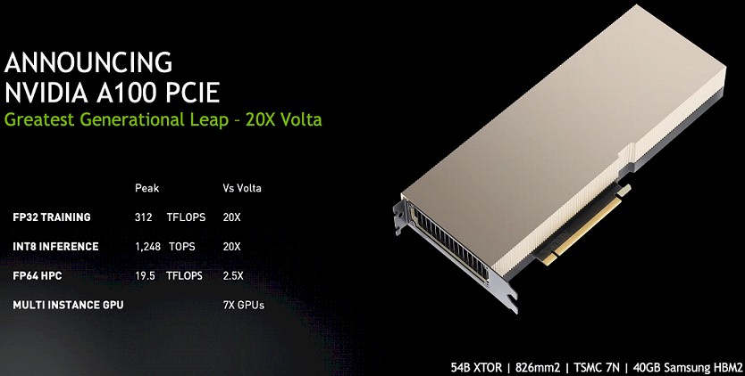
There is not a lot of difference between the SXM variant of the A100 and the PCI-Express card variant, except that the six NVLink ports on the SXM version can deliver 600 GB/sec of bandwidth into and out of the device while the x16 lanes in the PCI-Express 4.0 version can deliver only 64 GB/sec. To be fair, for those used to PCI-Express 3.0 peripherals, both will seem fast. It is also less costly to get the PCI-Express 4.0 version. Nvidia does not give out pricing on its GPU cards, of course, but we have worked with some resellers and system builders to get a sense of what old and new GPU accelerators cost on the market
We already went through the salient characteristics and performance using various data formats and processing units of Nvidia GPU accelerators from Kepler through Ampere in the architectural deep dive we did at the end of May. Now, we are going to look at the cost of Ampere A100 accelerators relative to prior generations at their current street prices. Ultimately, this is always about money as much as it is about architecture. All of the clever architecture in the world doesn’t amount to much if you can’t afford to buy it.
In the table below, we show the price, bang for the buck, and bang for the watt of the past four-ish generations of GPU accelerators (counting Turing as its own generation makes four in addition to the Pascal, Volta, and Ampere GPU accelerators). There are a lot of different performance metrics we can look at, and that is particularly true when considering sparse matrix support for machine learning inference. In this comparison, we assume the best case scenario using the various data formats and compute units as well as sparse matrix calculations when calculating performance per watt and performance per dollar. We also being it all together in the mother of all ratios, dollars per performance per watt, which is the be-all, end-all calculation that drives architectural choices at the hyperscalers and cloud builders.
Take a look at this table:
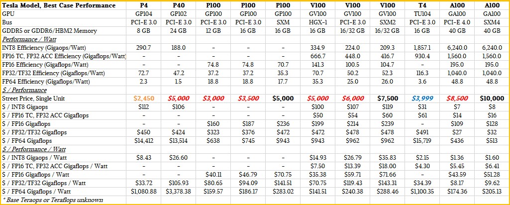
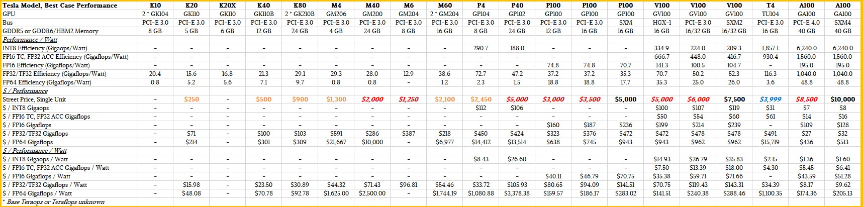
That’s just a subset of the data about server-class GPU accelerators from Nvidia that we have compiled over time. We have this big table that goes all the way back to the Kepler GPU accelerators, which you can view in a separate window here because it doesn’t fit in our column width by a long shot. This is the companion set for the two tables we did in the architectural dep dive, but as we said, now we are making performance fractions with watts and bucks.
Note: The dollars per performance per watt figures shown in this story’s tables originally had an error, which has been corrected. Apologies for that.
The first thing that we wanted to point out is that if the electric bill for your compute farm is paid for by another division or group at your company, then you might want to consider using Kepler-class K20, K40, and K80 GPU accelerators, which have street prices of $250, $500, and $900 a pop right now and which have the best FP32 and FP64 bang for the buck across six generations of GPU accelerators in the past eight years. We do not have historical pricing data for each and every one of these GPUs or we would show price/performance improvements over time.
What we can say since the Pascal generation is that performance and price/performance have generally improved and for a while there during the early Volta era three years ago, GPUs were in such high demand and in such relatively short supply that Kepler, Maxwell, and Pascal GPU accelerators were holding up in value more than you would expect based on the fact that Volta GPU accelerators were just so much better in terms of having more oomph and being more general purpose. This is how economics works, despite the best efforts of vendors who want to relegate their older products to the dustbin as soon as possible.
But eventually, new stuff has such a price/performance or performance/watt advantage that the old stuff has to lose value. This is happening, finally, with the P100 and V100 accelerators, in fact, which sell for around $5,000 and $7,500, respectively, right now in the SXM form factor. (You have to back out the cost of HGX motherboards and networking to get that based SXM price, and luckily some Nvidia partners helped us do that.) The A100 SXM, when you back it out of the DGX A100, has a street price of around $10,000 right now – a little bit less than the $11,500 that Big Blue was charging initially for these devices as part of its Power Systems AC922 supercomputer nodes when they debuted back on December 2017. That V100 SXM has lost 35 percent of its value in three years, as we think for a while there these V100 SXMs were selling for closer to $15,000 on the street because of demand. As best as we can figure, the PCI-Express 4.0 version of the A100 accelerator will sell for around $8,500.
Some things jump out immediately to our eyes in this chart. For one thing, no matter how much Nvidia loves the T4 accelerator for machine learning inference, any company that has to do both inference and training and that might also have database acceleration and HPC work as well is not going to buy separate GPUs for inference. With the sparse matrix support and running INT8 data through its FP32 units, the A100 SXM costs $8 per gigaops and the A100 PCI costs $7 per gigaops, and the T4 costs somewhere around four times as much per gigaops. The performance per watt is around 4X better, too, between the T4 and the A100 as well. And the T4 accelerator has very low FP64 performance, making it a poor choice, at just under $4,000 a pop, for running any HPC or AI training workloads that require 64-bit floating point. The T4 is 31X more expensive per unit of FP64 performance. It is only a good choice where only the smallest fraction of the workload is FP64.
There is a reason why Nvidia went with a more general purpose design with the Ampere, and this illustrates it well.
The other interesting thing to note is that the Volta V100 accelerators, whether PCI or SXM variants, have a slight premium per unit of work compared to their Pascal P100 predecessors. There is nothing odd about this, but it is a very slight premium in terms of performance per dollar. That’s the surprising part. And for INT8 workloads, the P4 and P40 accelerators based on the Pascal chips, which are in a PCI form factor, are also holding up pretty well and have not, as yet, lost all of their value in the market.
If you are going for strict bang for the buck and flexibility across data formats and crunching bitness, then the PCI version of the A100 accelerator is hands down the best of Nvidia’s GPUs right now if you use the TF32 format and also use sparse matrix support for integer operations. If your software doesn’t support these, you can you regular FP32, but the advantages are not as large.
One last thing to note: The gigaops or gigaflops per watt figures shown in our tables are at the device level, not at the system level. They are also peak theoretical performance and now sustained performance on a test such as the High Performance Linpack (HPL) or its AI variant, HPL-AI, benchmark test. So the gigaflops per watt figures are consequently much, much higher than what you see on, say, the Green500 rankings, which includes the whole system including networks and storage and its power and cooling.
How Nvidia Measures Bangs And Bucks
As part of the Ampere rollout, Nvidia released some HPC and AI benchmarks to give customers a sense of how real-world applications performance on the A100 accelerators and how they compare to the previous Turing and Volta generations as appropriate. Here is a market basket of HPC applications ranging from molecular dynamics – particularly important now with the hunt for a vaccine or treatment for COVID-19 top of mind – to physics, engineering, and oil & gas seismic processing.
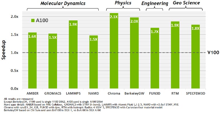
These are initial tests, and we have a strong suspicion that over time as the software engineers get their hands on Ampere accelerators and update their software, the performance will get even better. There is precedent for this, after all. Here is the performance over time of a market basket of HPC, AI, and data analytics workloads from 2016 through 2020 on the Pascal, Volta, and Ampere accelerators:
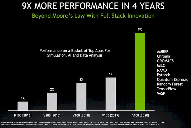
Now, we reckon that performance improvements in the AI stack, thanks to the use of increasingly mixed precision and the Tensor Core units, has risen more dramatically and is bringing up the class average. A lot of the gains in HPC have already been made by shifting from CPUs to GPUs and using technologies like GPUDirect, but there is now 64-bit processing on the Tensor Cores, so that gives 2X the performance over the plain vanilla FP64 units on the Ampere A100 accelerator. Our best guess is that the HPC applications in the chart above are not running on the Tensor Cores, so there is headroom for the software to catch up with the software and double the performance for these applications. So maybe when everything is all tuned up, it will be somewhere between 15X and 20X improvement on the same A100 hardware this time next year.
The important thing to note in that chart is how performance improved on the V100s with no changes in the hardware but lots of changes in the software, both in 2018 and 2019. There is no reason to believe that the features in the Ampere GPU will not be exploited to the hilt – eventually – by HPC software as much as by AI software. The stakes are just as high, and the software engineers are just as smart.
That brings us to AI by itself. The AI training models are getting more complex, with more and more layers of algorithms, both forward and backward propagation ricocheting like a laser beam before it comes out OF the mirror to cut through steel, and this is requiring an exponentially growing amount of compute. Like this:
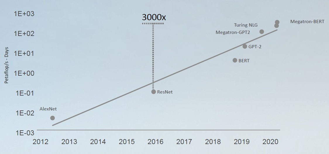
The test of choice for natural language processing, which is exponentially more complex than the image processing that was the benchmark of choice (ResNet-50 being the specific test) for the past couple of years, is the BERT test, which is short for Bidirectional Encoder Representations from Transformers. We told you about BERT last August, when Nvidia was positioning NLP as its next big AI workload, and one that would drive the requirements of devices like the Ampere GPU. BERT was, of course, developed by AI researchers at Google in 2018. The BERT-Large model had 340 million parameters is was chewing through, but Nvidia’s Project Megatron implementation of BERT scaled up to 8.3 billion parameters. ResNet-50 was handling a mere 26 million parameters to do its image processing. Bah.
In the architectural reference for Ampere, here is how Nvidia stacked up BERT performance for NLP training and inference:
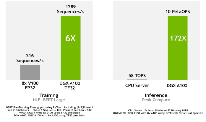
For training on the BERT-Large model, a DGX A100 server using eight A100 GPU accelerators linked by NVSwitch and using the TF32 format was able to process 1,289 sequences per second, compared to 216 sequences per second on a DGX-1 server with eight P100 accelerators operating with FP32 data in the FP32 units. That’s just a tiny bit under a factor of 6X improvement. Nvidia could have given inference numbers for the Volta or Turing GPUs here, but decided to compare to the most popular inference engine in the datacenter, the Intel Xeon SP CPU. In this case, a pair of Intel “Cascade Lake” Xeon SP-8280 processors running INT8 against a DGX A100 server with sparsity support enabled on the INT8 units. The Intel server could handle 58 teraops, while the Nvidia DGX A100 server could drive 10 petaops or 172X as much. (This appears to be peak theoretical performance.)
This chart, shown during the Ampere GA100 GPU launch, was explicit about BERT training and inference, normalizing performance for a single unit against that for the T4 and V100 where appropriate:
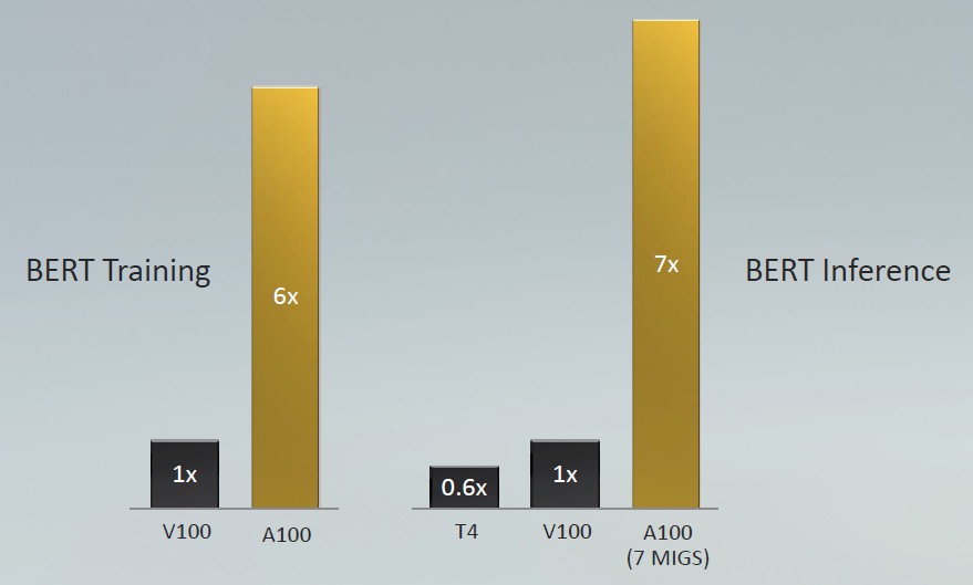
For BERT-Large training, the V100 was written in PyTorch and used FP32 precision, while the A100 used TF32 precision. (This is essentially the same data as above.) For BERT-Large inference, the T4 and V100 accelerators used FP16 operations, while the A100 used seven of the eight GPU slices (all that are currently turned on in any of them) and used INT8 with sparsity support turned on.
The upshot of all of this, according to Jensen Huang, Nvidia’s co-founder and chief executive officer, is that companies that are building AI training and inference systems can throw away a whole lot of CPU servers that are used for inference and converge the two workloads onto DGX A100 systems and be done with it. Here are the ratios that he gave out during the Ampere launch:
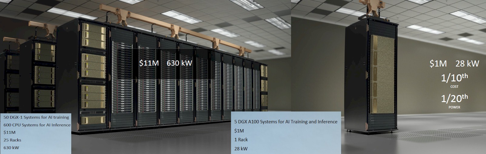
Now, as far as we know, it is very, very difficult to fully populate a rack with DGX A100 systems, or even DGX-2 systems, because of the compute density and as you can see from Nvidia’s own SuperPOD configurations used with its Saturn-V and Selene supercomputers, the company does not even half fill its racks for this reason.
“The DGX A100 server can be configured as eight GPUs for training or 56 GPUs for inference,” Huang told us at the Ampere launch. “All of the overhead of the additional CPUs and memory and power supplies and so on collapses 50 servers down to one, and it is going to be able to replace a whole bunch of different servers. This is going to unify that infrastructure into something that is more flexible and increases its utility and the ability to predict how much capacity you will need.”
More and more is a pretty good guess.

The Tough Road Still Ahead For Intel In The Datacenter
A few years back, when Intel went up on the rocks with its CPU and GPU designs largely because its chip research and manufacturing did not keep pace with the manufacturing and packaging advances made by foundry rival Taiwan Semiconductor Manufacturing Co, we said that we were rapidly moving towards …
Amping Up The Arm Server Roadmap
Competition in and of itself does not directly drive innovation – customer needs that might be met by some other product is really what makes suppliers hop to and get the lead out. No matter what you do in this world, there is always a chance that someone else will …
Intel Puts Its Xe GPU Stakes In The Ground
For about a decade, Intel has sold GPUs, in recent years with its integrated CPU-GPU devices used in client and entry servers. But for the most part, at its heart and despite acquisitions of FPGA and NNP makers, Intel is still a CPU maker. Nvidia and AMD have for years …
The more you buy. . .
. . . the more you save.
I don’t understand how to read your chart. In particular I don’t understand the $ per megaflops per watt. As an example, compare the FP64 of the T4 with that of the P40. The T4 has 3.6 Gflops/watt, which is 3600 Mflops/W. The P40 is less efficient at 1.5 Gflops/W, or 1500 Mflops/W. Now, the T4 costs $3,999 and the P40 costs $5,000. So the T4 both has a higher efficiency and a lower price, so it’s $/Mflops/W should be lower than that of the P40. However in your chart the T4 is said to cost almost 7 times the amount of money per Mflops/W, making it look like the P4 is a much better deal than the T4 for FP64 efficiency. However, the T4 is the better deal as it is both more efficient and costs less.
That’s because there was an error in the spreadsheet, which gave nonsensical numbers. It has been fixed. I blame working late at night for this error… Deepest apologies, and thanks for saying something.
T4 doesn’t cost $3,999 – it cost close to $2,000 (street price)
This is the price from HPE. And even at $2,000, A100 still beats T4 by a factor of 2X on price/performance.