

When you have 54.2 billion transistors to play with, you can pack a lot of different functionality into a computing device, and this is precisely what Nvidia has done with vigor and enthusiasm with the new “Ampere” GA100 GPU aimed at acceleration in the datacenter. We covered the initial announcement of the GA100 GPU and its Tesla A100 accelerator implementation two weeks ago, and now we are going to get into the architectural deep dive and then, of course, a thorough analysis of the price/performance of the A100 device compared to its predecessors in the Tesla lineup.
When we wrote our original story about the GA100 GPU and the A100 accelerator two weeks ago, the feeds and speeds of the devices were not all out, and subsequent to that announcement we have had several sessions with Nvidia, including a Q&A session with Ian Buck, vice president and general manager of the Tesla datacenter business, and a deep dive session with Jonah Alben, senior vice president of GPU engineering at the company. A lot of the details about the GA100 and its accelerator card are in the Ampere architecture whitepaper, which we are supplementing with material from these sessions and our own analysis.
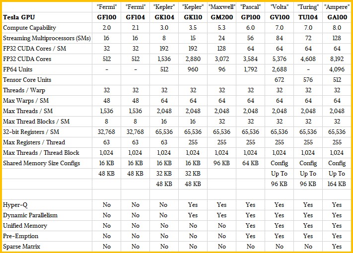
As with prior GPUs aimed at the datacenter dating all the way back to the “Fermi” chips a decade ago, which were the first in the true Tesla lineup, there is a hierarchy of compute engines, caching, and coordination logic in the Ampere design. The base organizing unit is the Streaming Multiprocessor, or SM, which has a number of different compute engines that sit side by side, waiting for work to be issued to them in parallel. This SM is what the HPC experts look at as the equivalent to a core in CPU land, for example when sizing up the “core” count on supercomputers in the Top 500 rankings that come out twice a year. Any collection of things behind the L1 instruction and data caches is a “core” to this way of thinking, and what Nvidia calls cores we might, in CPU Land, call a “unit.” (People from Nvidia sometimes call it a unit, too.)
In the old days, the elements within an SM were called variously Streaming Processors, or SPs, or CUDA cores, but these SPs now have a lot of different compute elements within them with different data formats and processing types, not just 32-bit single precision CUDA cores. Putting on our architecture hat, we think a credible argument can be made that each of the SPs within an SM should be considered a “core” as we know it, not the SM as others are doing it and very roughly and somewhat analogously to a core in CPU Land. It’s a finer point, we realize. What we care about ultimately is oomph per device, cost per oomph, and cost per oomph per watt.
An side: If you want to look at the history of the GPU architecture in Tesla devices since the “G80” chip that started off the general purpose GPU computing revolution, we did a big review of that back in February 2018 when we dove into the Volta GPU after talking to the architects at Nvidia.
Without further ado, here is what the Ampere SM and its four SPs look like:
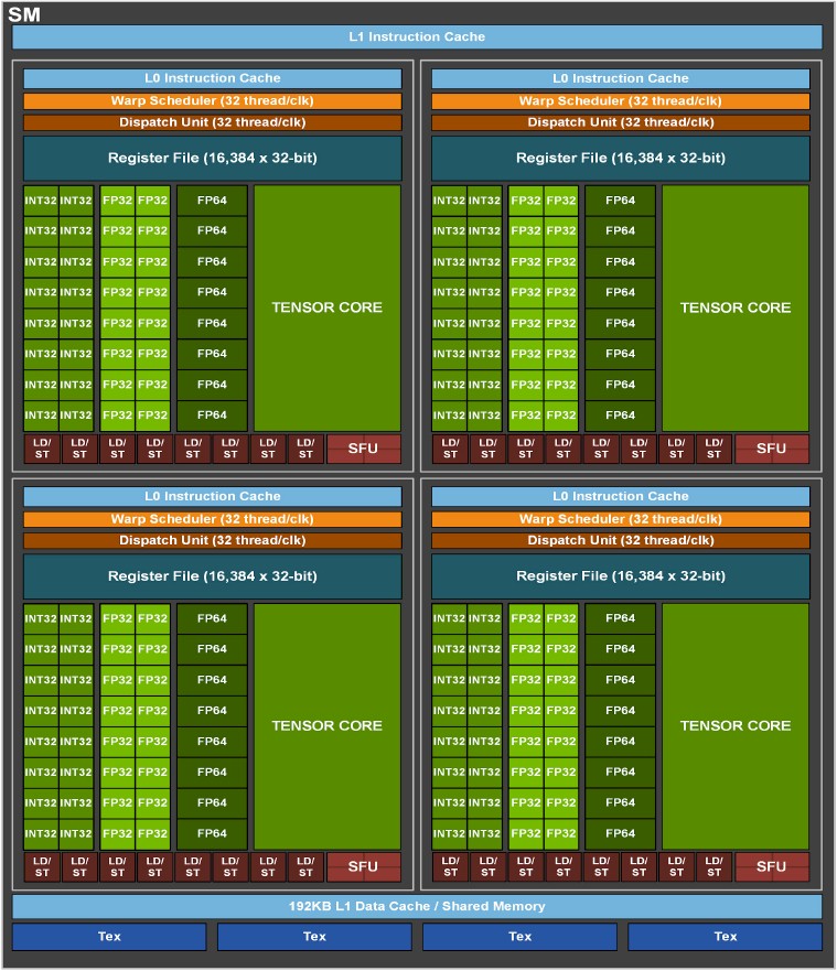
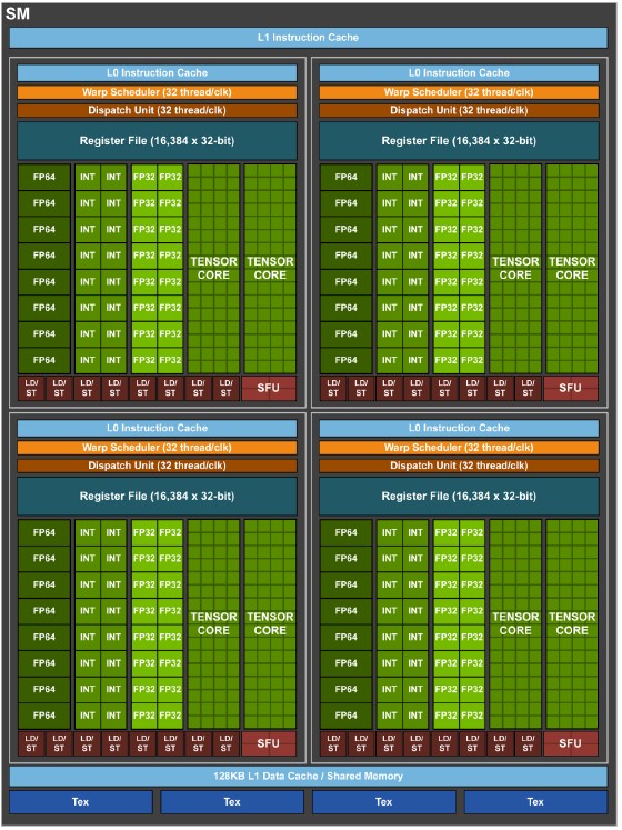
Each SP has sixteen 32-bit integer units (INT32), sixteen 32-bit floating point units (FP32), and eight 64-bit (FP64) units. This is very similar to the Volta SM. Like crazy similar, as you can see here:
We never did know the size of the Level 0 caches on Volta, and we don’t know the size on the Ampere GPU, either. But the feeds and speeds on the warp scheduler, dispatch unit, and register files on the Ampere SPs look the same as on the Volta chips. The L1 instruction cache sizes are similarly not revealed for the two devices, but we do know that the L1 data cache across the SM was 128 KB with Volta and is now 50 percent higher, at 192 KB, in Ampere. The load/store and texture units are essentially the same.
At a high level, Ampere is very similar to Volta, but there are a lot of tweaks in all of these elements of the Ampere SPs and the SMs that make them different in the details, such as the fusing of the pair of Tensor Core units in the SP to make them capable of doing a very high rate of 64-bit math. There are, as we have talked about already, a lot of innovations with data formats and sparse matrix acceleration that give high performance on AI workloads equivalent to doubling up the FP units or the Tensor Core units – to do so within the what is presumably about the same transistor budget. So don’t think we are not impressed. We are.
That sparse matrix acceleration, for instance, is a particularly neat trick, as shown below:
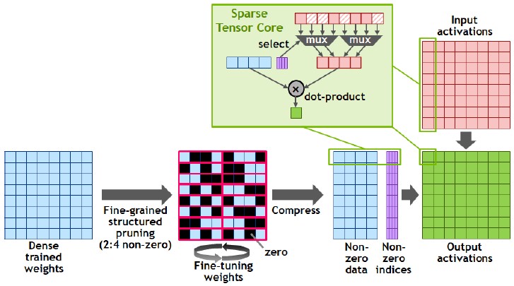
After a machine learning model is trained on the GPUs, there is a set of dense weights that are output by the model. Nvidia has created an automagic pruning technique that reduces the density of the matrix by half, using a 2:4 non-zero pattern, that does not result in the decrease in the effectiveness of the weights for inference, and by skipping the zeros introduced, the Tensor Core unit can do twice the floating point or integer math than it would have done with the denser matrix. We are not sure what happens with matrices that are already sparse, which happens with certain AI and HPC workloads. But presumably if they were using data in the right formats, these workloads could also see the 2X sparse matrix speedup.
The Volta chip had 84 SMs in total, with 80 of them exposed and four of them duds, which helped Nvidia get better chip yield out of the 12 nanometer processes from foundry partner Taiwan Semiconductor Manufacturing Corp, which were absolutely cutting edge three years ago. With the move to 7 nanometer processes at TSMC, the Ampere chip can have a lot more SMs on a chip, and in fact there are 128 in total. That is a 52.4 percent increase in SMs, and that is the big part of the improvement in performance moving from Volta to Ampere. The production Volta and Ampere devices had 80 SMs and 108 SMs, respectively, so at first this is more like an underlying 35 percent base increase in performance just from the increase in the number of computing units on the device.
Here’s what the fully loaded Ampere GA100 looks like with all of its 128 SMs:
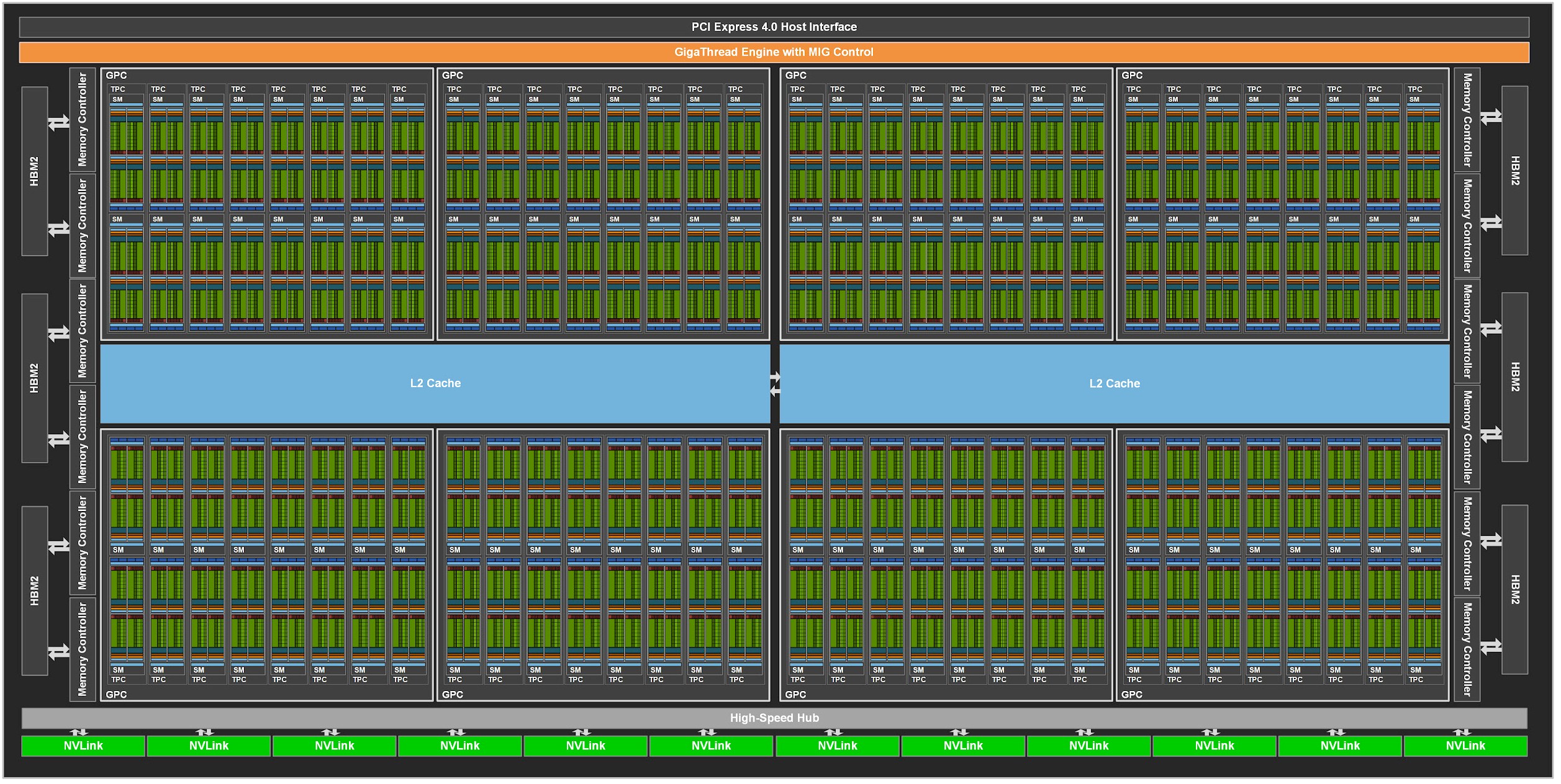
The hierarchy of compute in the Ampere GPU goes like this. Two SMs together comprise a Texture Processor Cluster, or TPC. Eight of these TPCs (and therefore sixteen of the SMs) comprise a higher level block called a GPU Processing Cluster, and eight of these make up the full GPU. That number is significant in that there are also eight Multi-Instance GPU, or MIG, slices that can independently be used as virtual inference engines and virtual GPUs for desktop infrastructure. The Volta GV100 GPU had six GPCs, which could have also been their own MIG in theory, but Nvidia did not allocate separate paths across caches and into memory controllers directly to each GPC in the GV100 as it is doing with the GA100. This is what a MIG really is – a more isolated and independent GPC – and it is a subtle change that nonetheless is an important one because it eliminates some of the contention for memory capacity and bandwidth when the device is being run as eight smaller devices instead of one big fat wonking one. This may be a subtle change, but it is an important one.
With the full arrays of SMs, the Ampere chip has 8,192 FP32 and INT32 units, 4,096 FP64 units, and 512 Tensor Core units. This is one hell of a dense device. With only 108 of the SMs activated, has 6,912 FP32 and INT32 units, 3,456 FP64 units, and 432 Tensor Core units that can run workloads.
There are some important changes with the Ampere jump from Volta. Starting from the outside moving in, the host interface is PCI-Express 4.0, which has double the bandwidth of the PCI-Express 3.0 interface used with the Volta, at 128 GB/sec duplex (64 GB/sec each way on an x16 slot with as the name suggests sixteen lanes).
That is not the only way into and out of the Ampere GPU. There are also the NVLink ports. With Pascal PA100 GPUs, NVLink 1.0 ran at 20 Gb/sec and each of the four ports on the devices delivered 40 GB/sec of bandwidth (20 GB/sec in each direction). With the Volta chips, Nvidia moved its signaling up to 25.8 Gb/sec for NVLink 2.0, which after encoding yielded 25 GB/sec of bandwidth per signal pair, for a total of 50 GB/sec each way and across six ports, that gave you an aggregate of 300 GB/sec of bandwidth into and out of the Volta GV100 chip. With Ampere, we think Nvidia is adding PAM-4, which adds two bits per signal and at 25 GHz gives each NVLink 3.0 lane the same 25 GB/sec bandwidth bi-directionally as NVLink 2.0, but it only requires half the number of signal pairs as NVLink 2.0 to give the same 50 GB/sec of bandwidth per port. So now the Ampere chip can have a dozen NVLink ports that still match the bandwidth of the NVSwitch port aggregation of 300 GB/sec, meaning there are some more interesting topological things that can be done to interconnect GPUs. (We will sort these out separately in a follow-on story.)
On the main memory front, there are a dozen HBM2 memory controllers that feed into six banks of HBM2 stacked memory on the GA100 chip. One ten of the controllers and five of these banks are fired up, giving the tesla A100 accelerator 40 GB of capacity and 1,555 GB/sec of aggregate memory bandwidth with the memory running at 1,215 MHz. The Volta chip launched with HBM2 memory running at 877.5 MHz and initially only had 16 GB of capacity and 900 GB/sec of bandwidth. The memory capacity was doubled up around a year later, but the bandwidth stayed the same, and in November last year at the SC19 supercomputing conference last November, Nvidia very quietly launched the Tesla V100S with only a PCI-Express 3.0 version and with 1,106 MHz HBM2 memory that boosted the memory bandwidth on the Volta chip to 1,134 GB/sec of bandwidth. To get to the performance it has attained, the V100S could have gotten there by having the remaining four of the SMs fired up, for the full 84 SM complement, boosting the performance across the board by 4.7 percent. But as it turns out, it has 80 SMs running at 1,601 MHz, an increase of 4.6 percent. This chip might have been useful in early 2019, and it is clear that some hyperscaler or HPC center needed a stopgap and got it. The Tesla A100 will step on it pretty hard.
If you compare the GV100 and GA100 block diagrams, you will see that the L2 cache on the Ampere chip is broken into two segments instead of the single L2 cache at the heart of the Volta chip. That L2 cache has been increased to 40 MB, which is a factor of 6.7X increase over the Volta chip. This is a big change, and we think that combined with the new partitioned crossbar structure that has 2.3X the L2 cache read bandwidth of the L2 cache on the Volta chip, this is a dominant factor in the raw performance improvements Ampere will shows over the Volta chip on raw performance on like-for-like FP32 and FP64 and INT8 units – without sparsity acceleration or new, more efficient numeric formats in the various units on the chip. And more precisely, what we are saying is that we think real applications will show a larger improvement than is expressed in the peak throughout figures for these base units, and then will get even more performance as they employ other numeric formats and move work from the FP32 or FP64 units to the Tensor Cores and accelerate even further.
For real workloads, we have to figure that Nvidia’s GPU architects reckoned that they did not have enough L1 cache and L2 cache to hide latencies in the GV100 chip and would be able to squeeze more of the inherent performance in the units in the Volta design by tweaking the memory hierarchy and extending it for Ampere. We think that the independent pathing that was done to create the MIG slices for inference and virtual GPUs for virtual desktops has also been a boon, creating a much more balanced engine for AI training and HPC. There are lots of other features that are adding to the increased performance, such as asynchronous copy, which loads data from the global HBM2 memory to the SM L1 cache memory without having to go through the register files.
Time, and benchmarking, will tell. It’s just a gut feeling we have.
Another thing to note. The clock speeds on the Ampere chips are actually lower than on the Volta chips, even with a sizeable process shrink from 12 nanometers to 7 nanometers. We don’t have base clock speeds, but we know the GPU Boost clock speed on the GV100 was 1.53 GHz when it was announced three years ago and it is 1.41 GHz with the GA100 today. So expanding the throughput of the base GPU through those additional 28 smaller SMs cost 7.8 percent in clock speed. This is not surprising. Raising clock speeds incurs too much power cost, and adding more concurrency is a better use of that power in all kinds of devices, including CPUs and FPGAs.
Even with the gearing back of the GA100 clock speed, the V100 accelerator weighed in at 300 watts, and the A100 comes in at 400 watts, or a 33.3 percent increase. Some of that is due to the HBM2 memory on the device of course, but we think that the GA100 chip is itself running a bit hotter than the GV100 chip, but it is hard to prove that.
Here is how the GA100 stacks up against the Pascal, Volta, and Turing GPUs used in Tesla accelerators in terms of features and performance on the widening array (pun intended) of numeric formats that Nvidia has supported to push more throughput on AI workloads through its GPUs:
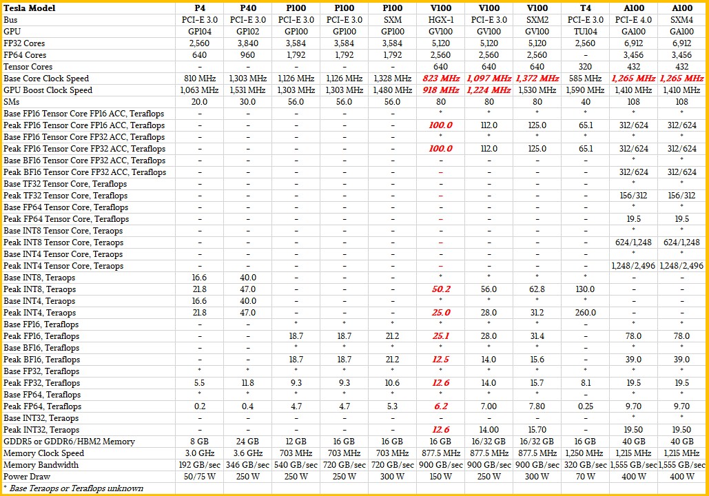
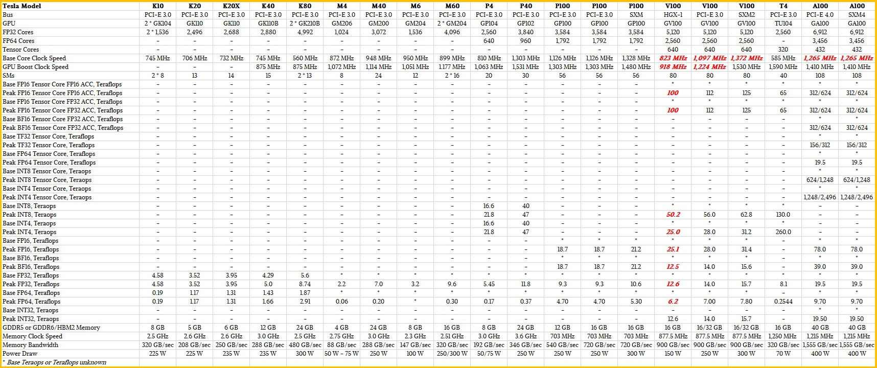
We have a bigger table that includes comparisons with the Kepler and Maxwell generations of Tesla accelerators, but this table is too big to display. (You can view it here in a separate window.) The FP16 with either FP16 or FP32 accumulate, bfloat16 (BF16), and Tensor Float32 (TF32) formats used on the new Tensor Core units show performance without the sparse matrix support and the 2X improvement with it turned on. The sparse matrix support also gooses INT4 and INT8 inference processing on the Tensor Cores by a factor of 2X when it is activated. It is not available on the FP64 processing on the Tensor Cores, but the Tensor Core implementation of 64-bit matrix math can deliver 2X the throughput on FP64 math compared to the FP64 units on the GA100 and 2.5X that of the GV100, which only had plain vanilla FP64 units. (We already compared and contrasted the BF16 and TF32 formats with others here.)
The base performance on the base FP64 units is illustrative when comparing the GA100 chip to the GV100 chip. It has only increased by 25 percent, from 7.8 teraflops to 9.7 teraflops, and that is just about the right ratio given the 35 percent expansion in the SM count and the 7.8 percent reduction in clock speed. That’s a 24.4 percent different in raw clocks across all the SPs in each device. (What we call Raw Oomph when talking about CPUs.) But, if you want to get double that performance, you can run FP64 matrix math through the fatter Tensor Core unit on each SP, and now you are at 19.5 teraflops across a GA100 GPU with 108 of its SMs and 432 of those Tensor Cores fired up. This performance gain did not come easy.
“It may not be obvious from the documentation, but is it’s a non-trivial exercise to get another 2X performance out of the SMs with the Tensor Cores,” Alben tells The Next Platform. “We pushed it as far as we thought we could in Volta without the thing catching on fire, but with a lot of hard work, we figured out how to get another 2X out of the system, and we were able to do that and get even better utilization than we did in the Volta generation. We are definitely proud to see the results.”
By the way, here is one thing to look forward to: That extra 20 percent of memory bandwidth and memory capacity will be unlocked, and so will the remaining 18.5 percent of latent performance embodied in the 20 SMs that are dark to increase the yield on the chips. This is a bigger block of latent capacity in the Ampere device than was in the Volta device.
Next up, we are going to do a thorough price/performance and performance per watt analysis of the tesla family of GPU accelerators, from Kepler through to Ampere. This is where the fun really begins, because you can’t talk about technology without talking about money.


Nice read!
You pointed out that the Tesla V100S is a fully-enabled GV100, but according to what I could find online, it is not the case, it is still a 5120-CUDA core/80-SM design. See for example, https://www.pny.eu/en/professional/explore-all-products/nvidia-tesla/1279-tesla-v100s-32gb
Finally, the last sentence of the paragraph mentioning the V100S is cut short… (“At some point, that other 8 GB of memory, an increase of”)
I got a bad steer from someone at Nvidia, and as it turns out, the clock speed and SM extension would yield the same result. Funny, that. Thanks for the help.
I’ve been wondering: why use the normal FP64 cores when the FP64 tensor units have double the performance? Do some applications just not run on the tensor units?
And also, would the HPL results for systems using the A100 GPU reflect the standard FP64 cores’ perfofmance or the tensor cores’?
Afaik the tensor cores implement less precise math than the shaders.
For clarification, a pcie gen4 x16 should get you 2GB/s per lane x 16 = 32GB/s each direction, ie 64GB/s full duplex…what is the total bandwidth that they support…?