

Arm server chip upstart Ampere Computing made a big splash with its 80-core “Quicksilver” Altra processor two weeks ago, and Marvell, which is the volume leader in Arm server chips with its “Vulcan” ThunderX2 processors (largely inherited from its acquisition of Broadcom’s Arm server chip assets), is hitting back with some revelations about its future “Triton” ThunderX3 chip and its roadmap out beyond that.
As we have said before, the roadmap for the years ahead is as important as the current design for all server compute engines these days, whether you are talking about CPUs, GPUs, FPGAs, or other kinds of accelerators. But compute engine suppliers also need a killer product right now, pushing the limits of architecture and process as hard as they can.
The Triton ThunderX3, which Marvell is talking about in more detail today, does just that, and it is doing it largely by throwing the thermal envelope out the window and letting the power go up as high as 240 watts for the highest end device. This allows Marvell to push up the clock speed and the core count, as well as adding more circuitry such as memory controllers and PCI-Express controllers, to keep those cores well fed. The Triton chip is a much beefier processor than many, including us, had been expecting – and largely because Marvell is designing for a much higher thermal envelope, knowing that at least some customers who want the most compute density as physically possible will pay for extra heat to have fewer physical servers to manage for a given level of serial and parallel compute. The Triton ThunderX3 chip is quite a bit bigger than you would expect given the feeds and speeds of the ThunderX1 and ThunderX2 (the Vulcan one, not the original ThunderX2 created by Cavium, which was acquired by Marvell, itself) processors.
We went through the history of the ThunderX family of server processors back in December, when the company’s top brass disclosed some features of the future Triton chip, and we are not going to walk through that all again. But it does bear considering that the original Cavium ThunderX chip from 2015 (when it started shipping) was etched in 28 nanometer processes from Globalfoundries and Samsung, and it had 48 relatively weak cores running at 1.9 GHz with a turbo boost up to 2.5 GHz. The follow-on homegrown ThunderX2 was expected to be etched in 14 nanometer processes (presumably from Globalfoundries) and to have 54 cores, but only six memory controllers, and that is why Cavium threw it out the window when Broadcom’s Vulcan design became available. The Vulcan ThunderX2 was etched in 16 nanometer processes from Taiwan Semiconductor Manufacturing Corp, and it had 32 brawnier cores with four-way simultaneous multithreading (SMT) in each core and a base clock speed of 2 GHz and a turbo boost once again to 2.5 GHz.
It was hard to guess what Marvell might do with a 7 nanometer shrink from TSMC, but it was clear from the US Department of Energy roadmaps for its Vanguard program of Arm-based supercomputers at Sandia National Laboratories that Sandia that the Triton ThunderX3 chip was expected to be installed during the fiscal 2019 government year, which started on October 1, 2018 and which ended on September 30, 2019. That clearly did not happen, but that is not all that much of a delay in the scheme of things and probably attributable to a change in foundry forced upon it by Globalfoundries killing off its 7 nanometer efforts back in August 2018. And it certainly is not significant compared to the delays that Intel has self-inflicted in its Xeon product line, mostly due to manufacturing issues with its 10 nanometer processes, which are akin to the 7 nanometer processes at TSMC.
Back in December, Gopal Hegde, general manager of the server processor business unit at Marvell, told us that ThunderX3 would drive a greater than 2X generational improvement in performance compared to ThunderX2. When pressed, Hegde added that the IPC jump combined with the clock speed jump from ThunderX2 to ThunderX3 was expected to be around 50 percent, which was a pretty big deal, and that L1 instruction caches and L2 caches would be expanded, too. Marvell would be tweaking arithmetic units, branch predictors, and other parts of the chip’s front end, and the cache hierarchy would be tweaked along with the prefetchers. And finally, clock frequency will go up, not down.
Our guess, given all of this, was that the top bin ThunderX3 part would have 64 cores, then that would be a 3X performance boost per socket with a higher clock speed and the IPC boost together. We guessed 20 percent for IPC and 30 percent for higher clocks (pushing up from 2.2 GHz to 2.9 GHz). We also guessed that if you geared the chips down a bit back to 2.2 GHz, you could drop the thermals a lot, perhaps back down to the 150 watts of the 32-core ThunderX2 instead of the 200 watts we expected from a 64-core ThunderX3.
The Feeds And Speeds
As it turns out, there will be a 64-core ThunderX3 part, and it may run at 2.2 GHz and it may fit in a 150 watt envelope as we expected, but the Triton chip is a much more impressive compute engine, topping out at 96 cores in a 240 watt envelope. Triton is a beast that is most definitely not only going to give Ampere Computing a run for the datacenter Arm server chip money, but it is also going to give AMD Epycs and Intel Xeons some very intense competition – at least for customers that largely control their own application software stack or who use open source software that has long since been ported to Linux on Arm.
Hedge tells The Next Platform that the Triton chip will come in variants with 32, 36, 40, 48, 54, 60, and 96 cores; we suspect that there could eventually be variants with 72 cores and 84 cores, but that was not mentioned in our briefing. The Triton chip is a monolithic design, and it is technically based on the homegrown Armv8.3 cores that Broadcom had created and that Cavium and then Marvell inherited through acquisition, with some Armv8.4 and Armv8.5 features brought in. The Triton family of processors will offer a range of speeds as well as core counts, and the salient features of the chips – memory controllers and PCI-Express controllers – will also scale up and down the line. The precise mix is obviously not being divulged right now.
The performance increase moving from ThunderX2 to ThunderX3 chips is going to be quite large. Across the product line, the instructions per core (IPC), which is a clock neutral measure of architectural performance, will rise by more than 25 percent, and the maximum turbo clock speeds will indeed rise by 28 percent, from 2.5 GHz to 3 GHz. In many cases, the clock speeds across the families will be the same, which is the case with the top bin 32-core ThunderX2 and the 96-core ThunderX3 chips, which both run at 2.2 GHz base clocks.
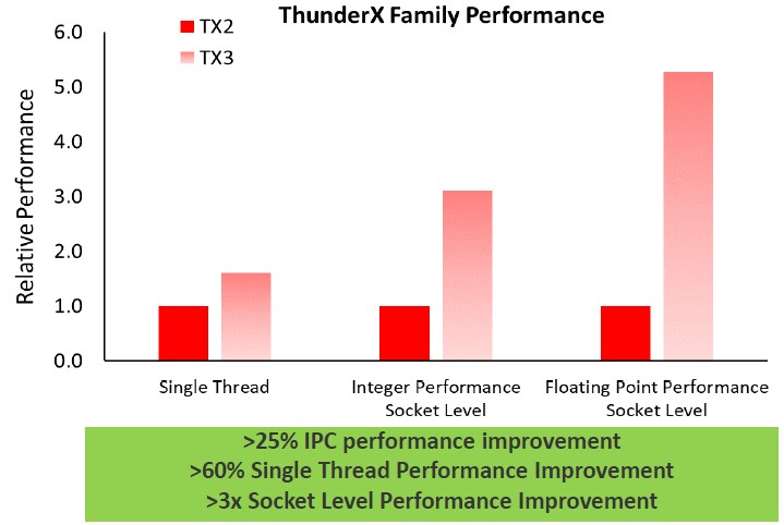
Notice how that base clock speed did not change for the top bin parts, so all the performance improvement in those chips is going to come from IPC and core count. So in that case, if the IPC was 26 percent (barely more than 25 percent) and the core count went up by a factor of three to 96 cores, and turbo was not really much of a factor, then the performance boost per socket would be on the order of 3.75X. The turbo boost function on Xeon SP CPUs is not for all cores at the same time, but it is for the ThunderX2 and ThunderX3 chips. Still, it is not clear how much headroom is in the 96 core ThunderX3 part for more gigahertz above that base 2.2 GHz clock speed. But a little boost could increase the throughput a bit more across that massive number of cores. We will find out when Triton launches.
“We took a desktop “Ice Lake” Core part and we benchmarked it, and based on what we know from some leaked roadmaps, we think we will basically be in the same range as Ice Lake Xeon SP in terms of single thread performance,” Hedge says. “We are using GCC as the baseline with standard compiler flags.” Obviously, there are compilers that Intel and Marvell both have to get architecture-dependent performance that is better than what GCC delivers.
The Triton chip will have eight memory controllers supporting memory running at 3.2 GHz, which is the same number of controllers in the Vulcan chip, which maxxed out at 2.67 GHz memory speeds. That’s a 20 percent increase in memory bandwidth, and the question is how that will balance out against the high core counts in some of the Triton SKUs. There are 16 PCI-Express 4.0 controllers on this chip, which have an aggregate of 64 lanes and therefore the same bandwidth as 128 lanes running at the older PCI-Express 3.0 speeds. The “Rome” Epyc 7002 series from AMD have 128 lanes per socket running at PCI-Express 4.0 speeds, so it is winning bigtime here. IBM’s Power9 chip has only 48 PCI-Express 4.0 lanes per socket, but it has high speed 25 Gb/sec SerDes for NUMA interconnect. The ThunderX2 chip had 14 PCI-Express controllers running at PCI-Express 3.0 speeds, so the I/O bandwidth increase is a factor of 2.3X greater for the ThunderX3 chip even if the lane count is only 14.3 percent higher. Unlike AMD, the ThunderX2 and presumably the ThunderX3 have dedicated Interchip Coherent Interface (ICI) circuits, now called Cavium Cache Coherent Processor Interconnect (CCPI), that implements NUMA coherency and links all of the cores and L2 caches across two sockets across the multi-terabit coherency fabric implemented on the Vulcan and Triton chips. The third generation of this NUMA interconnect has 24 lanes coming off each socket, running at 28 Gb/sec raw (25 Gb/sec encoded) each, which is exactly what IBM has in terms of speeds for the Power9 NUMA on-die interconnect. AMD has to burn half of the 128 PCI-Express lanes on an Epyc chip (both the “Naples” and “Rome” editions) to create two-way NUMA links between servers.
The point is, the ThunderX3 is not as light on PCI-Express 4.0 lanes as it might at first appear.
On the floating point front, there will be four 128-bit SIMD units on each ThunderX3 chip, which is twice as many as the ThunderX2 chip had, and these, days Hegde, will deliver more than 3X the floating point performance per socket. This is done by having higher clocks, some microarchtectural tweaks to keep the SIMD units better fed, and having twice as many 128-bit units. And while Intel has a 512-bit AVX vector units in its architecture, keeping it fed (it is more like a pair of 256-bit units) is hard and the clock speeds have to be reduced (by around 15 percent) when it is fully activated, and for some workloads, that second 256-but unit doesn’t get fed enough even if you turn it on. By the way, these vector units do not implement the Scalable Vector Extension (SVE) floating point format created by Fujitsu for its A64FX processor for the “Fugaku” supercomputer at RIKEN laboratory in Japan.
The Triton ThunderX3 chips will be sampling in the second quarter of this year, and it looks like from the roadmap that they will come out sometime early in the third quarter:
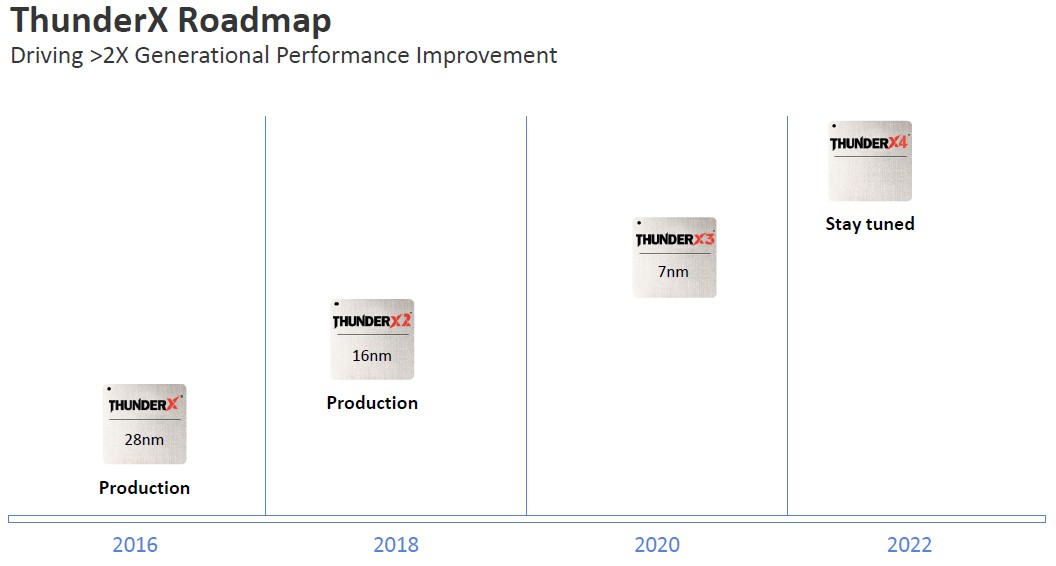
Marvell might be a little bit generous in this roadmap about when ThunderX1 went into production – we seem to recall it being in 2015 – and that makes the line look a little more straight than it is. But the company is thinking that a two-year cadence is sufficient, and is wondering how everyone else is going to go to an annual cadence and still innovate at a high level. ThunderX4 is, as this roadmap shows, in the pipeline for late in the first half of 2022, which could be about 20 months or so from now and which is probably based on 5 nanometer technologies from TSMC. Hegde says that it is doing early work on the 3 nanometer processes that are coming even later from TSMC, which gives it something to etch ThunderX5 with – possibly in late 2023 or early 2024 if you can draw a pattern from this data – and that is about as good as it gets for a roadmap horizon. No one else making CPU chips can see much beyond this point, either.
We will be following up with an analysis of the performance claims of Ampere Computing and Marvell regarding their respective Quicksilver Altra and Triton ThunderX3 processors.


Identifying competitive product and price voids in and around Intel product mix appears addressed but what about the ability to competitively supply?
Ampere, Marvell, adding AMD three questions arise are supply, combined supply volume and the market impact of supply volume grabbing sockets, racks, clusters, seats from incumbents. One has to wonder if some have changed their competitive ways or will continue to compete against each other? And isn’t there enough market for everyone?
How to supply production shops at best commercial price for lowest operating cost because in this market customers are price makers shopping for effective performance; availability, specifications, stability, utility values that get the job done and keep the business humming along.
No one’s going to risk the day to day business on anticipated or unanticipated effects of change. Innovation absolutely. Adoption, give it a try. But to put into production?
Business has infrastructure, market, financial and customer share to sustain.
Any among these three design producers in addition to IBM / Power can service specific segments to grow niche footholds into a stronghold, but how not to get trapped there, surrounded by Intel associate complex on proven ability to supply whole product in volume.
Volume on economies of scale and cadence commensurate with production shops building out, upgrading, burning through then literally throwing away or brokering off infrastructure that is truly commodity hardware to do it all over again.
There is no stretch just churn.
Intel continues to produce Xeon volumes well in excess of data processing and network communications real time demand. Currently those products, Skylake / Cascade Scalable are just good enough and at a dirt cheap pricing keeps business humming along . . . until this generation of product is scraped for infrastructure’s next volume feed.
Data processing is key, fast switching definitively key, light and aggregated and heavy tasks where an incumbent network feeds computers on businesses need to keep markets alive and prospering.
Question remains, who will supply volume capable of feeding this machine commensurate with keeping established business humming along.
Time to market is on the horizon? Have markets ever changed?
Mike Bruzzone, Camp Marketing
I wonder what the thunderX3 96 core will cost? I’m not hearing much on the tx3 IO. I thought Mellanox held the industry record internet speeds through various medium.
“Obviously, there are compilers that Intel and Marvell both have to get architecture-dependent performance that is better than what GCC delivers.”
Presumably you mean something like “[…] architecture-dependent performance in benchmarks […]”?
I’ve not seen many Linux servers use icc binaries in production.