

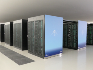
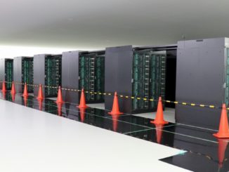
When it comes to energy-efficient supercomputing, sometimes less is more. That was illustrated this week by Fujitsu with its A64FX prototype, which captured the top spot on the Green500 list. The machine has no accelerators, network cards, or main memory on the motherboard. Everything has been sucked onto the processor package.
As is evident from its name, the A64FX prototype is equipped with the Fujitsu chip of the same name, and the one that will be powering the upcoming “Fugaku” supercomputer at RIKEN lab in Japan, a fact that has earned it the nickname micro-Fugaku. The prototype is essentially a two-rack, 768-processsor version of its much larger brother.
According to the new Green500 rankings released this week at SC19, the prototype delivered just a skosh under two petaflops on the High Performance Linpack (HPL) benchmark and did so with just 118 KW of power. That translated into an energy efficiency rating of 16.9 gigaflops/watt, which was just enough to capture the number one spot on the new Green500 list.
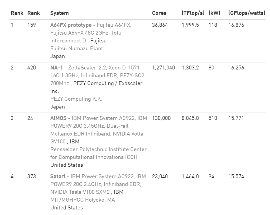
The lack of an accelerator makes the prototype an extreme outlier. For the past several years, the upper echelons of the Green500 has been dominated by supercomputers outfitted with these PCI-Express coprocessors, mostly of the GPU persuasion. The last time a non-accelerated system made it to the number one spot was June 2012, when an IBM Blue Gene/Q supercomputer captured the title.
Even on the current Green500 list, all the systems between the top-ranked A64FX prototype and TaihuLight, at number 35, are equipped with accelerators. But TaihuLight is about one-third as efficient as Fujitsu’s machine, with a Green500 result of 6.1 gigaflops/watt. It’s powered by the 260-core ShenWei 26010 processor.
The A64FX processor is a 64-bit Arm implementation developed by Fujitsu and RIKEN that uses the Scalable Vector Extension (SVE) technology. In a sense, the A64FX’s 512-bit SVE unit acts as an on-chip accelerator, since it can deliver about 3 teraflops at double precision on its own. That puts its double precision floating point performance in the general vicinity of a GPU. The speediest Volta V100 GPUs from Nvidia delivered 7.5 teraflops when it was announced in May 2017 and has been tweaked in recent years to push that up to 7.8 teraflops. The “Vega 20” CPU used in AMD’s Radeon Instinct MI50 and MI60 accelerators run at 6.7 teraflops and 7.4 teraflops, respectively. But they all need about 300 watts to hit those peak values. A closer analogy is the now-orphaned Intel “Knights Landing” Xeon Phi processor, which was launched in June 2016, also delivers 3.46 teraflops, but draws 245 watts in its peak configuration. Clocking it down a bit and turning off some cores cuts the price by 20 percent and reduces throughput to 3 teraflops, but in a 215 watt thermal envelope. Faster is not always better.
The A64FX tops out at about 170 watts, which is a good deal more power efficient than the Xeon Phi, but not as efficient as the current crop of GPUs. Of course, GPUs need a host processor and a PCI-Express connection to the host, elements that an A64FX-based system is able to dispense with.
So what makes the A64FX machine so green?
Although some people believe the Arm architecture is inherently energy-efficient, that’s not the case. If it were, then the Astra supercomputer, which uses the Marvell ThunderX2 Arm processors, would rank a lot higher on the Green500 than number 176, where it currently sits.
According to Toshiyuki Shimizu, the Senior Director of the System Development Unit at Fujitsu, the efficiency of the prototype system is the result of both hardware and software innovations. The hardware side centers on the A64FX itself, which is made using the 7 nanometer FinFET process and 2.5D Chip-on-Wafer-on-Substrate (CoWoS) packaging technology from Taiwan Semiconductor Manufacturing Corp to integrate Fujitsu’s Tofu D interconnect and main memory.
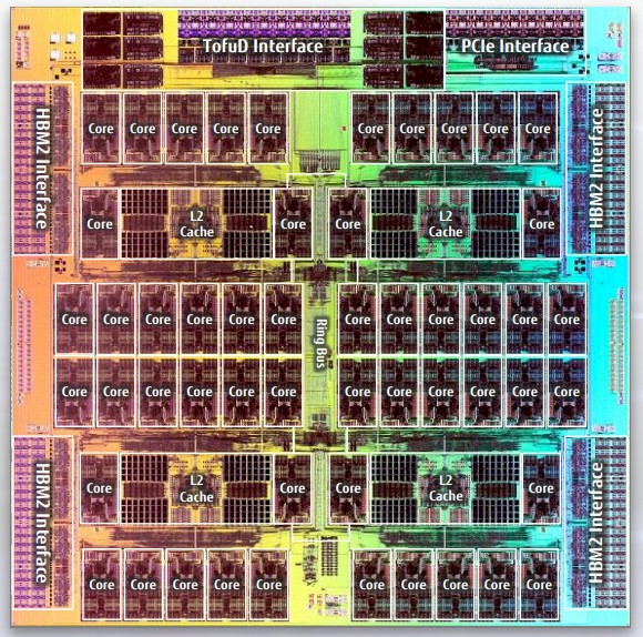
The A64FX is one of three HPC architectures that put all of their main memory on the package, in this case, in the form of four 8 GB HBM2 modules. NEC’s Aurora vector engine uses HBM2 memory as well, and the predecessor Sparc64-XIfx processor from Fujitsu used Hybrid Memory Cube memory from Intel and Micron Technology. The Knights Landing Xeon Phi processors used a mix of MCDRAM on package from Intel, a riff on Hybrid Memory Cube, and DRAM on the system board. With the Fugaku system architecture There is no DRAM sitting on the motherboard. As a result, less power is used to drive bits to and from memory, since the four HBM2 modules are sitting right next to the processor on the package instead of at the end of a wire in the form of a DIMM. Depending on who you believe, HBM2 is between 3X and 10X more energy efficient from a bandwidth perspective than DDR4 memory.
It’s worth pointing out that 32 GB of memory is somewhat on the low side for an HPC node these days, even for a single-socket system like the A64FX machine. DRAM chews up a fair amount of power, so systems with more memory tend to be less energy efficient, all other things being equal. Most systems today are using 128 GB per node, albeit for two sockets. A system somewhat analogous to the prototype is the Oakforest-PACS system built by Fujitsu the University of Tokyo and the University of Tsukuba in Japan, which uses a single 3 petaflops Xeon Phi processor per node. But in this case, in addition to the 16 GB of on-package Xeon Phi memory, there is also 96 GB of conventional DDR memory. GPU accelerators tend to have 16 GB or 32 GB these days, and they offload to host memory when they can.
The A64FX on-chip Tofu D interface undoubtably saved a few watts, since a network adapter plugging into the single PCI-Express 4.0 port on the system would draw more power. In general, integrated interconnects are uncommon, since they add complexity and can limit choice, but the advantage of on being on-chip not only makes for better energy efficiency, but potentially better network performance as well.
On the software side, Shimizu said that their long experience with the Tofu interconnect enabled them to fine-tune the communication libraries for extra efficiency. Likewise, for the math libraries, which they were able to optimize for the A64FX SVE instruction set. The Fujitsu team also did performance tuning on the HPL code using a set of analyzer and monitor tools.
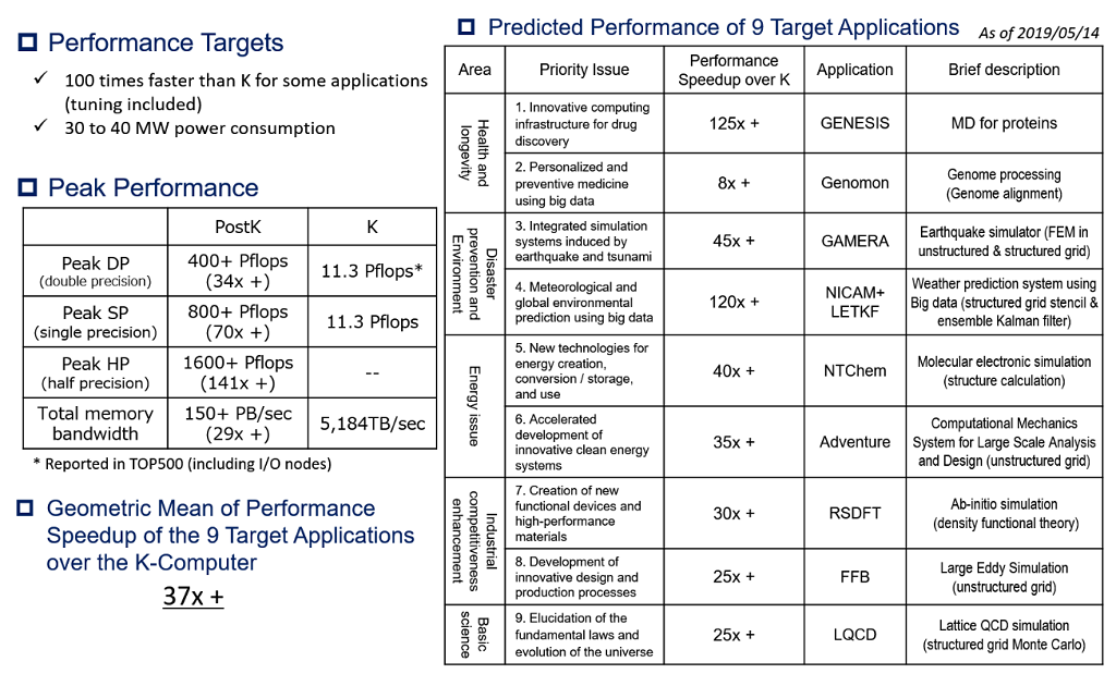
As impressive as the prototype’s energy efficiency is, the technology would require nearly 60 MW to deliver an exaflop on HPL. Since the plan is to not exceed 30 MW to 40 MW for Fugaku, it looks like they are only going to be able to scale this system to about 400 petaflops – that according to the current performance specifications of the system from RIKEN’s website. At this point, the performance goal is to be able to run key applications one or two orders of magnitude faster than they ran on the now-decommissioned K computer, a system with a peak performance of 11.3 petaflops.
Will the A64FX create an appetite for non-accelerated HPC machines? We may soon find out. The processor will be offered in commercial products from Fujitsu in the form of their new FX1000 and FX700 systems, as well as in Cray’s CS500 line. The test case is imperfect, since the A64FX also has to fight the headwinds of Arm adoption in a market untested for this architecture. But if the chip manages to hit the right balance of performance, programmability, energy efficiency and price, chipmakers and their customers may rethink the utility of accelerators.

Fujitsu Cloud Service to Put Fugaku Supercomputer in Reach
For those looking to try out Fujitsu’s Arm-based PRIMEHPC FX1000 system, the company is opening up the same capabilities via its own cloud service. Access to the Fujitsu A64X-based systems, which are at the heart of the top-ranked Fugaku supercomputer in Japan, will begin in October in-country, with global rollout …
Isambard 2 Is About Driving Technology Diversity
It’s been just more than a decade since Arm executives began to talk about bringing the company’s system-on-a-chip (SoC) architecture, which has long been the dominant design for processors found in billions of smartphones and other mobile device, into the datacenter. They boasted that within years they would be chipping …
With Fugaku Supercomputer Installed, RIKEN Takes On Coronavirus
Supercomputers are designed for a number of big jobs that can only be done by massively powerful machinery, and one of those jobs has been the modeling of chemical compounds and biological systems, often in concert to model diseases and to help find cures for them. The “Fugaku” exascale-ish system …
SVE is the reason why this design is more energy efficient. Given that it’s part of the Arm architecture it can be claimed that it’s a more efficient architecture (for these classes of workloads) as a result.
A lot of the energy efficiency here comes from the frugal compute core, but a lot is from the integration. Not having to drive the ddr memory bus, not having to pass data around the pcie interconnect, even the torus network topology is optimized to use short copper cables instead of integrated optics. It’s very clever. I’m still concerned that the efficiency of HBM is offset by the restrictions it places on the codes that the system will be able to run. With that little memory per core, there is no way you can run an mpi rank on every core, even for modest sized codes; the message passing tables would leave no space for the actual code to run. This machine can run HPL at incredible efficiency, but can it run productive applications for science, and with what programming modal?