

The rapid changes underway in modern datacenters and HPC environment are demanding more compute power from a tech industry that is running into significant barriers to supplying that capacity. There are few people on Earth who know this fact better than Lisa Su, president and chief executive officer of AMD.
Despite the slowing of Moore’s Law, devices are proliferating, huge amounts of data are being generated that needs to be processed and analyzed and processed, so much so that we have used machine learning to teach the computers to do it because human beings and the sequential code they write cannot keep up. Artificial intelligence, data analytics, software-defined storage, and immersive computing – they all demand more compute power, Su explained in her keynote at the Hot Chips conference at Stanford University.
“The key message in all of this is no matter which of these applications you’re talking about, you need more compute to progress,” Su said. “Forget about whether Moore’s Law is alive or dead. That’s an interesting conversation. But the more interesting thing is applications need for us to be above Moores’s Law. We need to do more than the industry has done in the past because the applications and data are such that there’s a lot more computation that’s necessary.”
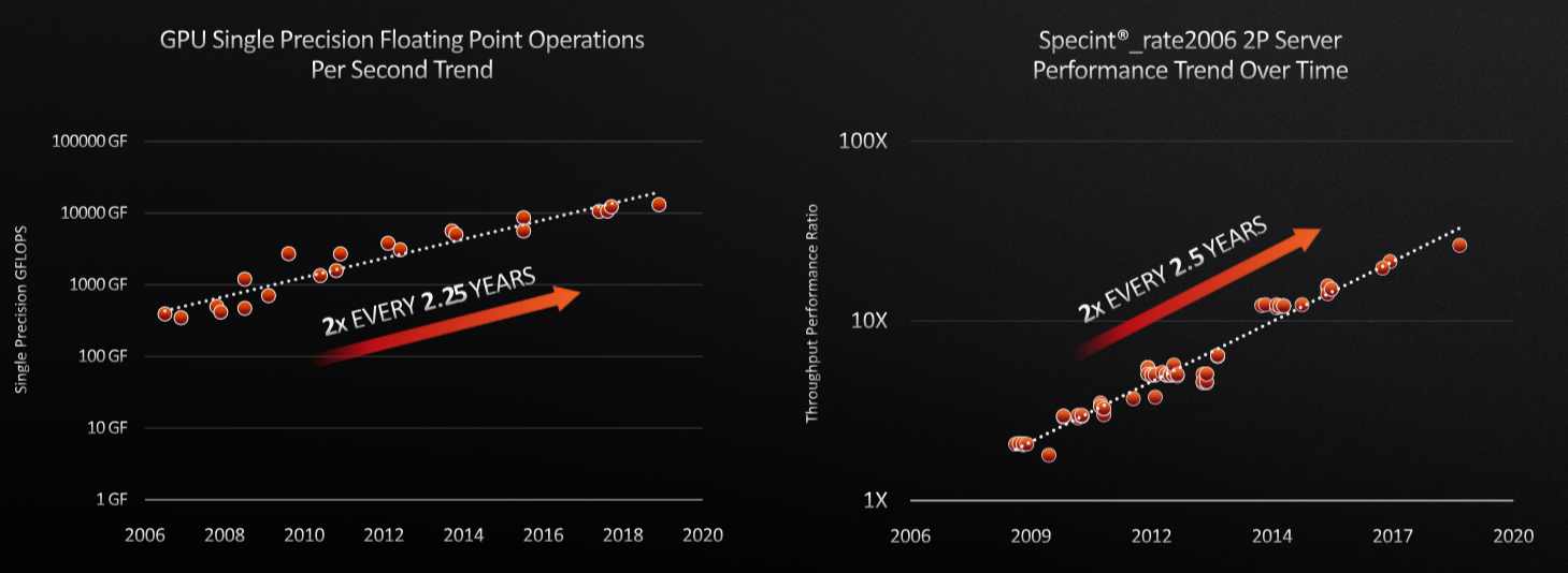
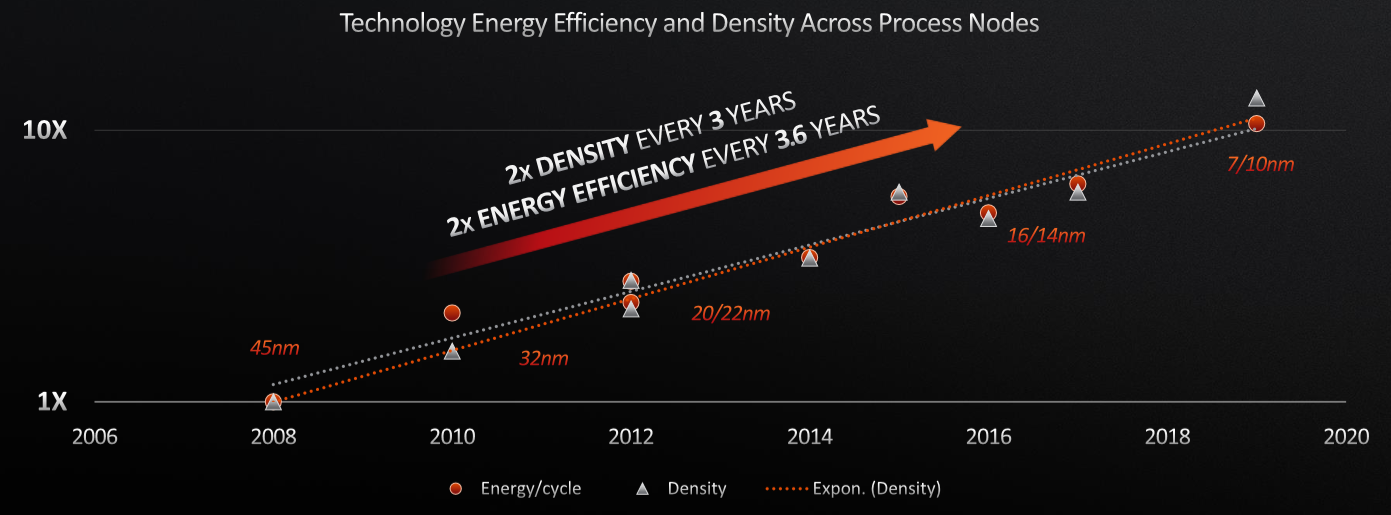
This is easier said than done, of course. Over more than a decade, CPUs and GPUs have steadily gained twice the performance every two-plus years while transistor density has doubled every three years and energy efficiency has taken nearly four years to do so. Take a look at the data Su presented. Here’s the floating point and integer performance for two socket servers since 2006, which is when the public cloud really started to take off:
And here are the transistor density and the power efficiency trends:
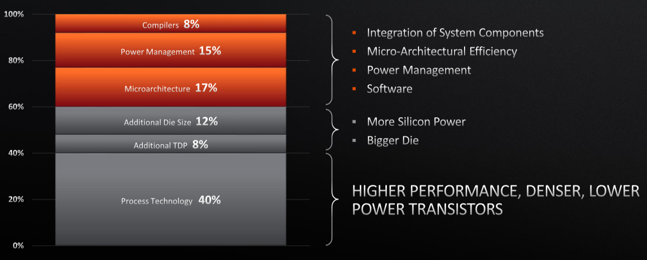
Yet there are things that need to be done to keep or extend the performance curve, with process technology accounting for about 40 percent of the effort over the past ten years, die size and additional TDP accounting for another 20 percent and the mircroarchitecture, power management and compilers making up the rest of the picture.
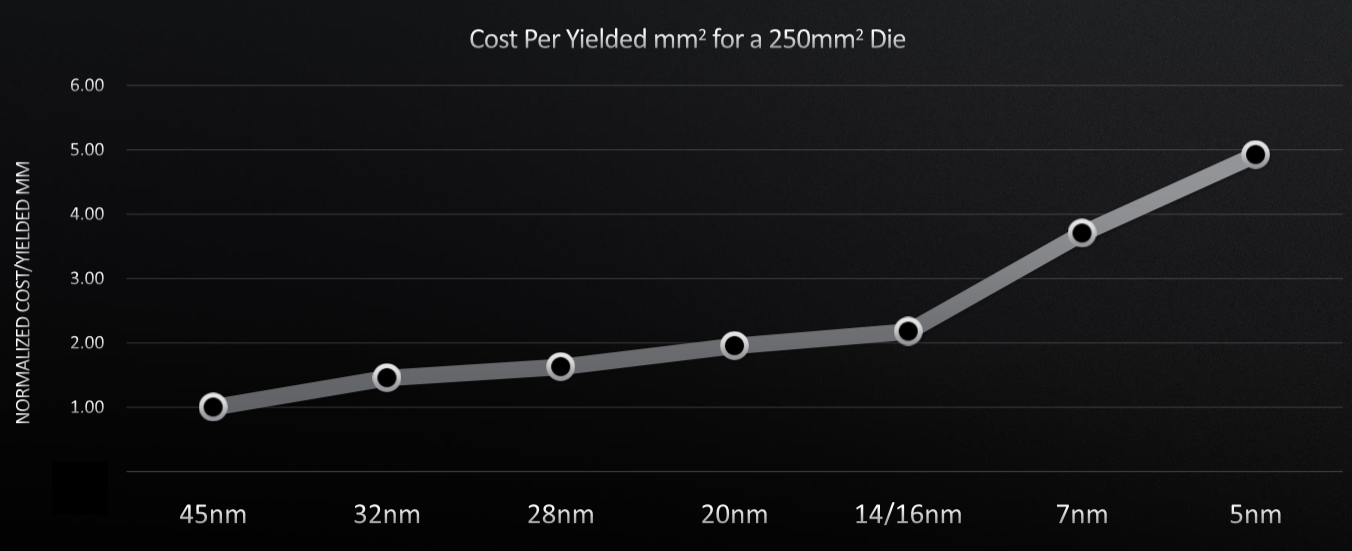
It’s getting more difficult to tweak each vector for high performance computing – in the general sense, not meaning just simulation and modeling – with barriers like the slowing of Moore’s Law and rising costs as the die size increases. Here’s the Moore’s Law curve:
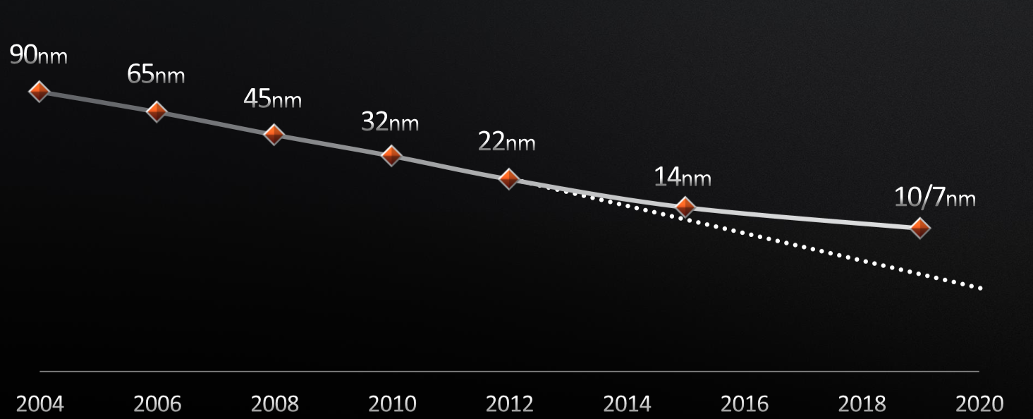
The curve is bending up as you can see as successive nodes take more time to come to market, and at the same time – in a not precisely causal way – the costs of bringing chips to market is rising as development and software costs rise and the engineering and manufacturing equipment costs for each process shrink comes out:
The irony is that back when AMD was talking so enthusiastically about power efficiency in the Opteron era when it had an edge over Intel’s Xeon processors, companies running datacenters did not care as much about that as raw performance. But now, all processors, no matter how much you integrate stuff with a system on chip design, come with substantial power and cooling challenges.
“The idea that power has become sort of the first order of optimization really came about over last seven to eight years, but we keep pushing the envelope,” Su said. “On our highest performance processors as well as our competitors,’ we keep trying to push the envelope on power. We’ve gotten better in terms of cooling technologies and cooling capabilities, but still you’re only increasing power an order of high single-digit percentage every single year. We’ll keep trying to push the envelope on power, but you reach some important physical limits on how you can cool silicon.”
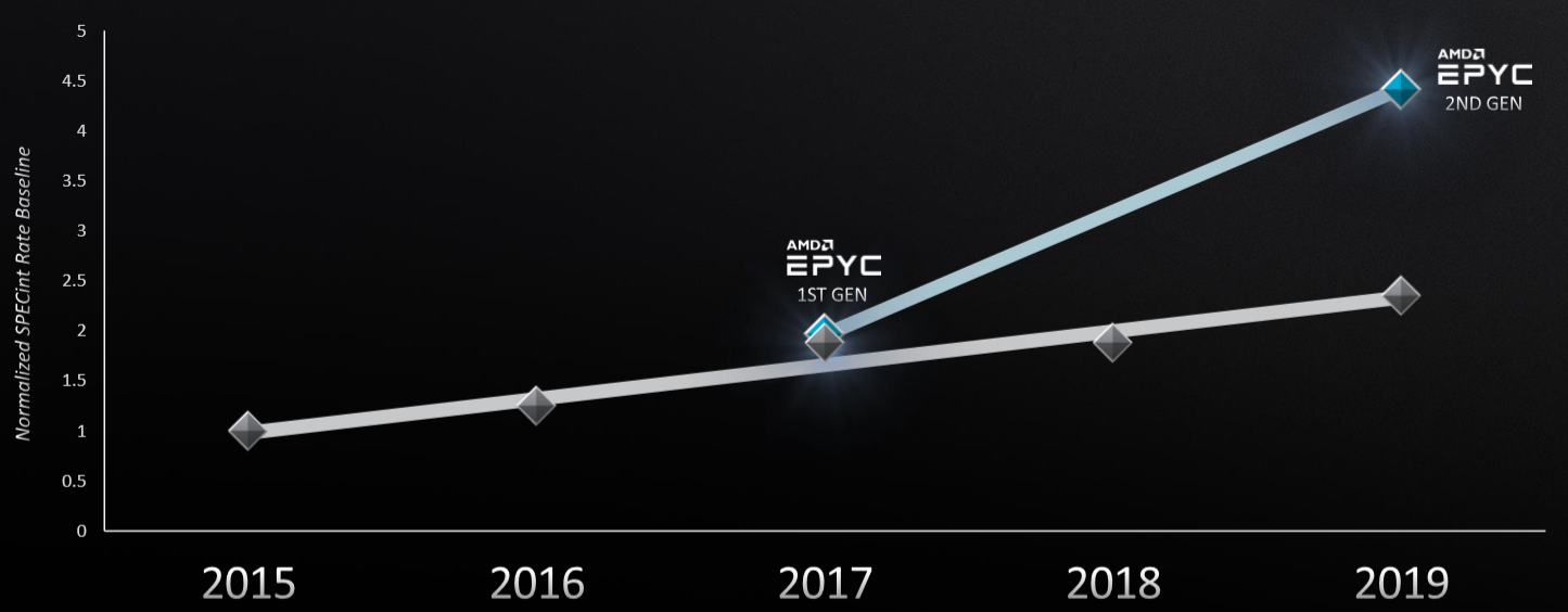
AMD engineers took all of that into account when they developed the company’s Zen architecture, which debuted in the first Epyc server processors in 2017, followed by the launch of the second-generation Epyc “Rome” chips and the Zen 2 architecture earlier this month. You can go to The Next Platform for a deep dive into the new chips as well as a look at the expanded portfolios OEMs like Hewlett Packard Enterprise, Lenovo, and Dell are rolling out powered by the next-gen Epyc chips.
At Hot Chips, Su turned to the design and architectural work AMD did with Zen 1 and Zen 2 as examples for what the industry needs to do to keep up with the growing demand for more compute power while overcoming the barriers inherent with traditional chip efforts. Generally speaking, it meant looking at the challenge holistically, not just with the silicon but also the system and software, developing a microarchitecture optimized for the workloads they’re running and creating an ecosystem of partners. It also meant looking down the road at upcoming generations of products to ensure that they continued improving performance and keeping costs in check.
“We saw those two trends in the 2013 to 2014 timeframe,” Su said. “We said, ‘Something has to change.’ You cannot just keep doing bigger and bigger monolithic chips. You can do it, but you just won’t get the performance, so we made a big investment in multichip architectures.”
That meant leveraging chiplets on a multi-chip module, a design that undertook a significant change from the first-generation Zen architecture to the second.
“The idea of this was to get more bang for your buck,” the CEO said. “It was to ensure you got more performance at a better cost points, so we got better yields by using a smaller die. With that, we had a nice architecture. As we migrated to 7 nanometers, we enhanced this idea of chiplets to really try to optimize the right transistor for the right technology. In the second-generation Epyc, which was just launched recently on both our desktop processors as well as our server processors, we decided that the most valuable transistors were the CPU, so those we’ve done in 7 nanometers. But the I/O and memory, which frankly weren’t scaling all that well, we’ve actually done in older generation technology, in 12 nanometers. So what you see with that is each IP is in its optimal process technology. You actually get a very nice architecture and it breaks some of those trends, and frankly, it gives us a ton of flexibility. With the same basic design, we can go across high performance desktops, you’ll see this in high-performance workstations and in high performance severs. It’s an example where innovation around chiplet architecture really gives you bang for your buck going forward.”
The result was a significant gain in performance over standard industry trends.
System design was equally important as silicon design, Su said. The key is understanding the applications that are being run and then being able to optimize both the silicon and system. Silicon is important, but systems need more than general-purpose CPUs. There are GPUs, field-programmable gate arrays (FPGAs), and custom ASICs, and different applications will need different ratios of each. Heterogeneous platforms also call for high-speed interconnects between the nodes – the Rome chips use PCI-Express 4.0 – and an advanced Infinity Fabric architecture.
Silicon vendors also need to understand software and applications if they are going to deliver the performance needed for modern workloads.
“No matter how we look at it, we as silicon guys need to make sure that our silicon is as programmable as possible to deliver optimal system performance,” she said. “From that standpoint, there is a whole bunch of stuff on the order of ‘get the most out of your silicon.’ We’re trying to get the libraries, the profilers, debuggers, compilers, all of those things as optimized to silicon as possible. But we also believe very, very strongly in an open source environment to sit on top of its so that everyone can contribute to this.”
For example, when developers are using TensorFlow or PyTorch for machine learning applications, silicon makers have to ensure that their products are optimized for that software.
Machine learning of an application that is driving the need for more compute power. CPUs and GPUs are doubling in compute capabilities every two or so years. However, the rapid demand for more training for machine learning algorithms is doubling compute consumption every 3.5 months.
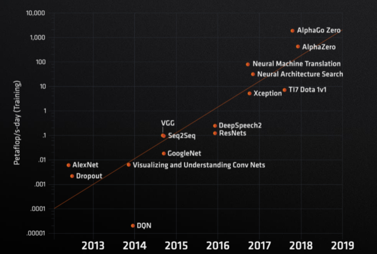
“It’s actually a mind-boggling thing,” Su said. “What that means is you can come up with these great algorithms and ether you take an incredibly long time to figure a problem out or you build large, large compute farms or you try to get more efficient compute and you probably do a little bit of each of those things.”
The performance of the supercomputers, as embodied in the Top500 rankings of machines, is another example of a challenge to be addressed. The supercomputers are still getting faster, doubling every 1.2 years, but the rate is slowing. Here is what a classical HPC application, in general is doing:
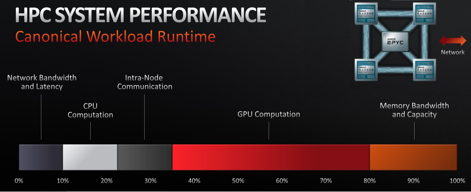
Innovation is needed to get the curve back on track, and offering systems optimized for particular workloads is key. But it is important not to over-generalize, and Su made the point with this data comparing a traditional HPC workload and a more modern AI one, both of which can run on similar GPU-accelerated systems:
![]()
In the chart above, the two HPC applications have different compute needs, with the NAMD application for molecular dynamics being GPU-intensive while the machine learning application for natural language processing needs more CPU capabilities than you might expect.
“My point in showing this is anyone who tells you, ‘If you just do this, everything’s going to be perfect,’ that’s just not the case,” the CEO said. “You have to do it all. You have to optimize CPUs, GPUs, the interconnect, the memory as well as network bandwidth together to really push the envelope in HPC.”
Given all that, she noted that there is a lot of work being done around CPUs and GPUs, but innovation in connectivity is not keeping up at the same pace. The same can be said about memory bandwidth, which also is lagging.
“Although we’re continuing to invest in very, very close coupling between the memory and the computing element, memory bandwidth over time is not really keeping up,” Su said. “We are big believers in high bandwidth memory. High-bandwidth memory has a strong roadmap that is important to continue on an aggressive pace. We also look at a lot of optimization within the die so the on-die cache hierarchy can have a larger impact on these memory bandwidths. But as we go forward, you can imagine that 3D stacking or other integration methods will help us extend this memory bandwidth curve as we need it to over time.”
Su noted that many of these optimization efforts will be on display when “Frontier,” the 1.5 exascale supercomputer being built by AMD and Cray (which is being bought by HPE for $1.3 billion) for Oak Ridge National Laboratory, rolls out in 2021. It will have highly optimized CPUs and GPUs, a coherent interconnect between the two and low latency node-to-node capabilities. It also will be able to run not only traditional HPC workloads but also commercial applications leverage AI and machine learning. Eventually many of the technologies in the system will make their way down into more commercial systems, Su said.
We definitely believe that. And that is how it is supposed to work.


So, is Moore’s Law breaking down or not? And if it is, is there anyway around it? Simple answers please.