

Earlier this week we focused on the entry of FPGA maker, Achronix, and their strategy to tackle the high end of this market with a datacenter-focused, 7nm device expected to emerge later this year. As a follow-up to the introduction we wanted to dive into what makes this a unique approach and how it might challenge current devices from dominant Xilinx and Intel/Altera—at least at this early stage.
Key to the architecture of the standalone Speedster7t is the company’s network on chip (NoC) driven architecture, something that takes a definite sharp turn from existing FPGAs, certainly from Intel’s integrated reconfigurable approach and also the most powerful Xilinx devices.
As we noted in our introduction to the company, there is a heavy emphasis on strategizing around where the two dominant FPGA makers are either failing or have not focused heavily enough. There is a somewhat limited application space to chase for high-end datacenter use cases in compute and networking but Achronix is unique in its heavily strategy-focused team. We talked to Manoj Roge earlier this week who has been gauging the ins and outs of the ecosystem for both Altera and Xilinx. The company’s Steve Mensor, whom we spoke to for the technology deep dive here, has a similar background with over 25 years in FPGA circles, most recently as Sr. Director of Marketing at Altera.
Mensor unpacked the reasons why starting from scratch with an FPGA design with specific focus on a few workloads is critical and how the NoC is key to making FPGAs more efficient, if not for all workloads, certainly for their initial datacenter targets in AI in particular.
“We started with a clean slate because what good is all the efficient compute in the world without the ability to feed the beast? We design the right memory hierarchy and bandwidth balance from an external memory (DDR4 for deeper buffering and GDDR for high bandwidth versus expensive HBM) and on-chip memory. We wanted to move data efficiently—that was our first focus.”
Their approach began with what amounts to building another layer of routing, which compared to something like a high-end Xilinx Versal part with communication links, is more akin to a big mesh between the major constructs (the CPU complex, vector engines, and the FPGA). The goal was to move data between those blocks versus across the FPGA fabric.
As seen below, Achronix built a “row and column” routing structure that sits above the FPGA with full access via what the call NAPs, or network access points.
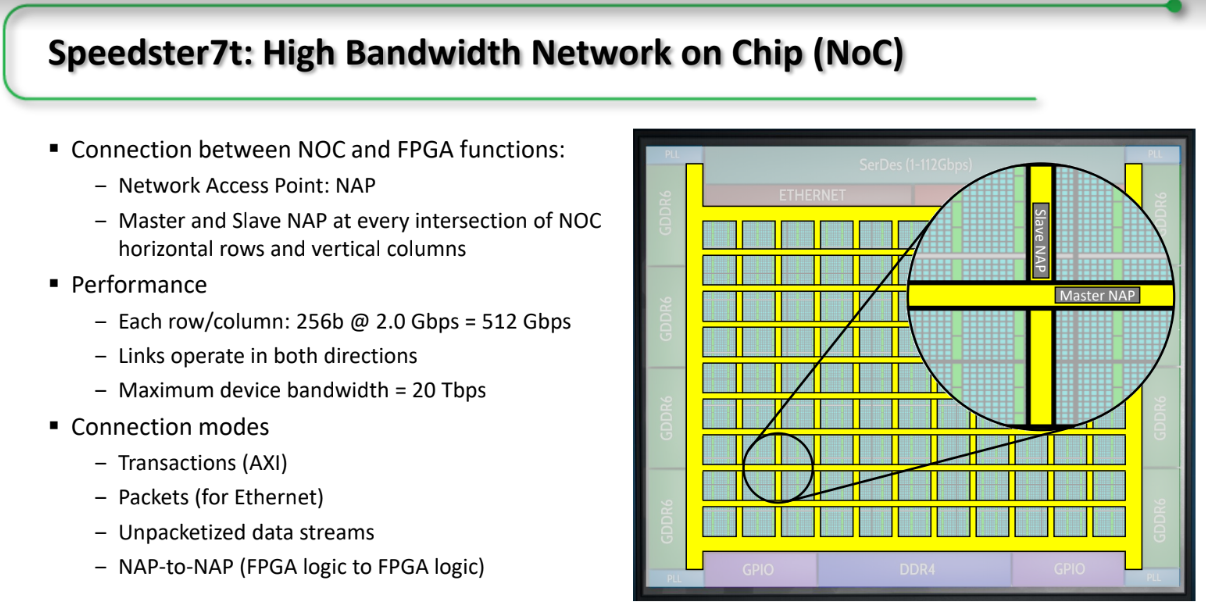
The NoC talks to all surrounding I/O (PCIe, Ethernet, DDR, GDDR) along these paths. Each runs at 2GHz at 256 bits wide (512Gb/s). Compare this to devices on the market that run at 128 bits at 1GHz (one-quarter the bandwidth per link).
It is important to point out that these rows and columns are not a switch network. These are more like streaming pipelines. The horizontal rows fly over the vertical columns so it is not possible to zigzag (although Mensor says there are ways around those if someone is really serious about it). This stream across the fabric without switching, something Achronix says is one of the biggest innovations in FPGAs in years. “It is simply not possible to do this if you don’t have a ubiquitous array of these NAPs. They are not intersections or crossover points; there is a slave NAP and a master NAP. This is compared to what exists now with connect points in the vector engines or in the CPU complex or small number of locations in the FPGA. Our intent was to change the current design thinking and focus on this kind of data transfer,” Mensor explains.
There’s never a free lunch, so what’s the catch? The easy answer here is that Achronix took a hit in silicon area. But Mensor says this was an “investment for benefit. It’s a hardened ASIC NoC architecture with programmability to get to the fabric via the NAPs” and is a suitable price to pay for the data movement and efficiency benefits.
Even though all the functionality is in the FPGA device, the challenge is making it all work, especially if you want to build a couple of accelerators and get those to work as a system. You need to hook into memory ports, configure the memory in the FPGAs, hook up the clock, which is where things get harder when you’re driving the data in and doing clock domain crossing and synchronizing. These are not difficult circuits but it is hard to close timing on an FPGA. The challenge is in the switch matrix would have had to build. One that could address memory and the accelerator with no guarantee of available memory or accelerators, which means building further arbitration in both directions. It just gets very complex,” Mensor says. “The whole circuit grows quadratically in an FPGA so when you add another accelerator the switch circuitry that goes with it more than grows linearly. It’s also a performance bottleneck and challenging (see red area in chart below—a lot of overheads that adds to real value to the circuit).
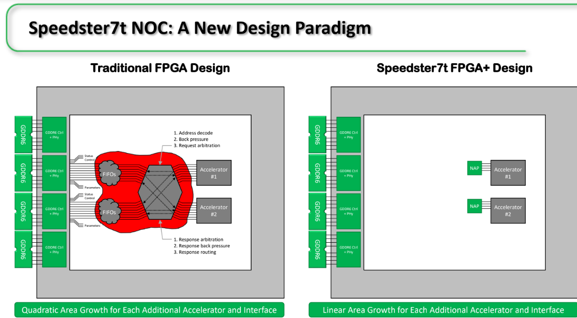
This is why Achronix says their device is suitable when building systems with multiple FPGA accelerators (say one for encryption and another for encryption). The engineer designs a first accelerator, then a second, then all that is needed is to hook it into NAPS. “This is similar to software where the OS takes care of all the functionality in terms of memory mapping, drivers, virtual machines, almost everything so the software person doesn’t have to think about hardware. Of course, this time, the hardware is doing the work so for the first time in FPGAs we don’t have to think about making everything fit into a hardware construct. The accelerator design work is done in Verilog or VHDL, it is hooked into the NAP and the hardware takes care of everything else.”
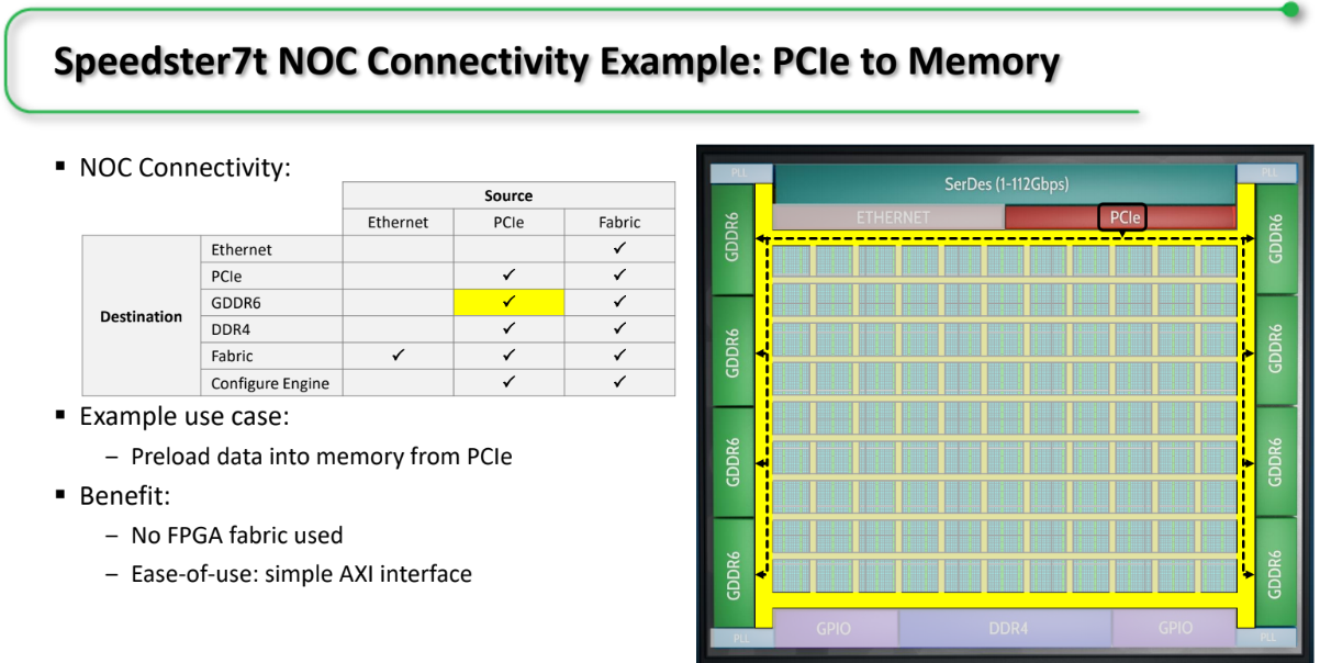
To put all of this in some practical context, Mensor shared an example case. Above the user wants to host data from the host processor as fast as possible through PCIe to the memory and use the high-bandwidth memory to communicate with the accelerators. In this case it is possible to go through PCIe through the NoC directly to get to the GDDR controllers connected to the on-board components. The moral of the story? None of the FPGA is involved in the process. The ASIC implementation is hard-coded through the NoC so there’s no step with Verilog or VHDL, it’s just a matter of telling the chip how to load the data.
Another scenario is when two accelerators are talking to each other. FPGA #1 does encryption, the second does compression. The architecture means it’s possible to address accelerator #2 and have a high-speed direct path “without the floorplanning since it’s modular.”
“It eliminates the long, congestive routing needed with lots of accelerators and also eliminates the switch network. This means there is just a mesh to avoid congestion and remain close to the highest speed points as per place and route. It is possible to always design smaller circuits in an FPGA but the challenge is when those grow in quantity and have to work with all the other functionality efficiently in a system.”
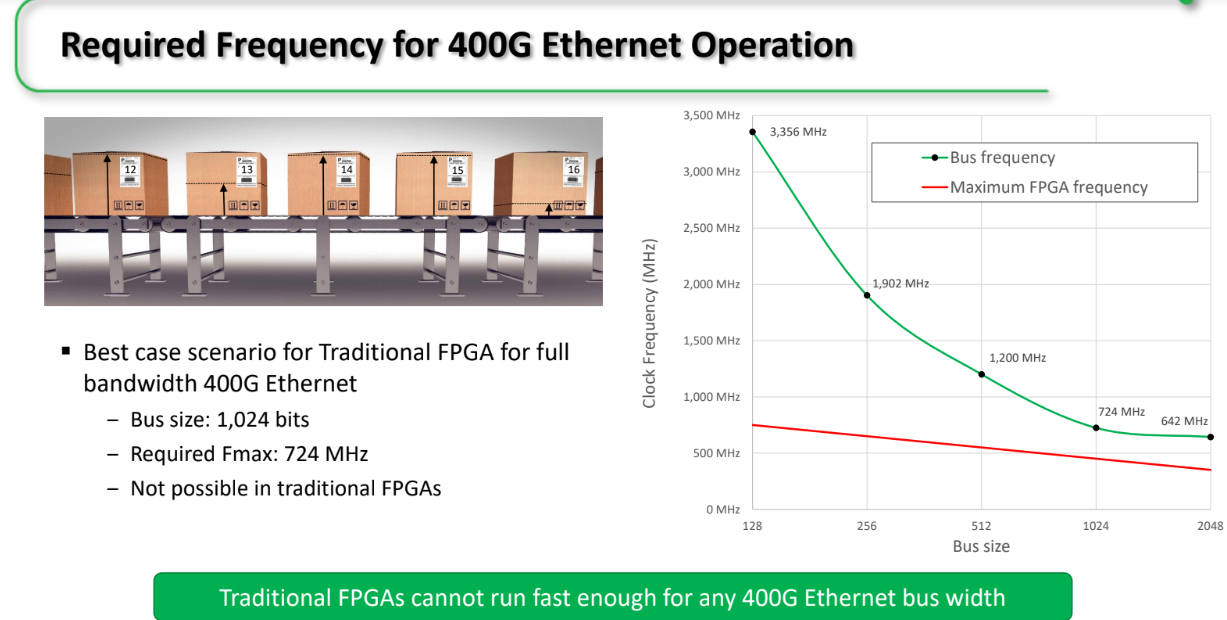
Another unique feature is the ability to approach 400Gb Ethernet. Below on the right is the case of an ASIC, FPGA, or any device. The green line shows the tradeoffs between frequency/bus size and drives home the impossibility of doing much at all with 400Gb Ethernet on an FPGA (that’s a big can of worms you can open for a wider view).
See how Achronix sees the 400G story for FPGAs—or at least its Speedster7t below.

On the left is general device with 1,024-bit bus at 724 MHz. With their NoC’s dedicated circuitry for Ethernet packetized streaming they are arguing 400G is possible by breaking that 400G into 100G streams that can be anywhere delivered by a 256-bit bus running at 506 MHz, something that is possible on a 7 nanometer device. The point is, the NoC and some special circuitry means high performance data transfer that might not be possible without this NoC mesh.
We will keep a close eye on the FPGA space as it pertains to datacenter workloads (compute and network acceleration). That’s been pretty easy since there are not many tackling the high-end space. We are keeping Achronix on our watchlist to see where this finds a home. Their site has some impressive ResNet and AI workload benchmarks but the real test in our minds is when the MLperf inference-focused results emerge later this summer.

A Cornucopia Of Memory And Bandwidth In The Agilex-M FPGA
When it comes to memory for compute engines, FPGAs – or rather what we have started calling hybrid FPGAs because they have all kinds of hard coded logic as well as the FPGA programmable logic on a single package – have the broadest selection of memory types of any kind …

Xilinx Benefits From Intel FPGA Shortages
As AMD is getting closer to closing its $35 billion acquisition of FPGA maker Xilinx, it is natural to think about how well that business is doing and how it is competing against its main rival, Intel – specifically, the Programmable Solutions Group, formerly known as the free-standing Altera before …

Reimagining Accelerators with Sparsity at the Core
There could be a new era of codesign dawning for machine learning, one that moves away from the training and inference separations and toward far less dense networks with highly sparse weights and activations. While 2020 was peak custom AI chip, it could be that the years ahead feature devices …
Be the first to comment