
In theory, customers running HPC simulation and modeling applications want to cram as much compute in as small of a space as they can. In practice, the situation is a lot more complex because workloads are changing as AI code enters the fray and accelerators – particularly GPUs but also FPGAs here and there – are increasingly used even if plain vanilla CPU computational engines are the norm.
HPC centers have to weigh a lot of different factors when it comes to choosing their next platform, and the job is not getting any easier with the widening SKU stacks at Intel, particularly with the “Cascade Lake” Xeon SP processors announced two weeks ago and the competition coming from IBM Power9, AMD Epyc, and Marvell ThunderX2 processors as well as Nvidia Tesla and AMD Radeon Instinct GPU accelerators.
Sorting out the best motor to base an HPC cluster upon is more complex than calculating a raw cost per unit of floating point performance because price, memory bandwidth, and thermals also have to be taken into account. This is a lot of data to gather and synthesize, and we are going to do our best to help with that process, starting with the initial comparative benchmarks that Intel has put together to compare Cascade Lake-SP and Cascade Lake-AP processors, the latter of which cram two whole processors into a single socket to double up the density of a two-socket machine, to prior generations of Xeon processors and to AMD’s initial Epyc X86 server chips, code-named “Naples,” announced nearly two years ago. These comparisons come as AMD is readying its second generation “Rome” processors for market, and AMD is eager this time to take on Intel’s Xeons to run traditional simulation and modeling workloads.
For those customers who bought first generation “Skylake” Xeon SP processors, also announced nearly two years ago, there really is not a lot of reason to move on up to Cascade Lake processors of any kind, particularly given the fact that HPC centers tend to keep their systems for three, four, or sometimes even five years. But some HPC shops add nodes to existing machines, and those who have clusters currently running on “Haswell” Xeon E5 v3 from 2014 or “Broadwell” Xeon E5 v4 processors from 2016 will be able to add a lot more flops to their boxes and expand their clusters, or replace the whole shebang if that is how they want to roll.
Given this, it is not surprising that Intel’s first benchmark tests pit a two-socket machine based on its Broadwell Xeon E5-2697 v4 processor, which has 18 cores spinning at 2.3 GHz, against two-socket machines based on its mainstream Cascade Lake SP-8260 Platinum processor, which has 24 cores running at 2.4 GHz, and on its doubled-up Cascade Lake AP-9242 Platinum processor, which has 48 cores running at 2.2 GHz. There is a three year gap between these machines, which is when the upgrade cycle starts happening at a lot of HPC shops.
Here is how Intel stacks up these three machines running a variety of HPC benchmarks, including base CPU tests as well as codes commonly used in weather modeling, manufacturing, life sciences, and financial services:

None of the chips shown in the chart above are the top bin parts in their respective lines. They are processors that HPC customers who are looking for a reasonable amount of performance and reasonable bang for the buck might choose as the compute engines in their clusters.
On the STREAM Triad memory bandwidth benchmark, the Cascade Lake SP-8260 is delivering about 60 percent better performance thanks in some measure to the extra compute but mainly due to the Skylake and Cascade Lake chips having six DDR4 memory channels rather than the four in the Broadwell and earlier designs; the Cascade Lake-AP system has two chips per socket, so it has twice as much memory capacity and bandwidth per socket (if all of the memory channels are filled up, of course). The memory in the Cascade Lake systems is running at 2.93 GHz, compared to the Broadwell chip at 2.4 GHz, which helps on the memory bandwidth.
Given that the Broadwell Xeons supported 256-bit AVX2 floating point engines and the Skylake and Cascade Lake chips have 512-bit AVX-512 engines, it is no surprise that on raw Linpack matrix math or on the computationally dense and memory bandwidth intense HPCG benchmark that the plain vanilla Cascade Lake system delivers 1.73X the Broadwell system on HPCG and 2.19X on Linpack. Given that the Cascade Lake-AP system has two chips per socket running at almost exactly the same clock speed as the Cascade Lake-SP system, it is also no surprise that the quad-chip, two-socket Cascade Lake machine has double the performance of the regular two-socket, two-chip Cascade Lake-SP system. This is so by design – it is really a quad-socket system in two-socket clothing, after all.
In general, as you look across these HPC workloads, the plain vanilla Cascade Lake-SP machine delivers about 1.9X performance compared to the Broadwell system tested, and the Cascade Lake-AP delivers 3.7X. Our guess is that the Cascade Lake-AP system costs twice as much, and the bang for the buck is not all that different. Dell, Hewlett Packard Enterprise, and Lenovo, the three biggest server OEMs who would normally have pricing and configuration information on new Xeon systems have not launched Cascade Lake-AP machines, and have no plans to at this time except if customers do a special bid, so we have no idea what the system cost looks like. But we have a hard time believing that the bang for the buck will go up much, if at all, compared to a regular two-socket server using the Cascade Lake-SP system. This is a density play, for the most part, and a machine that Intel launched so it could show performance leadership in a “two-socket” server.
No matter. The point is, customers with clusters based on Broadwell Xeons will be able to see a big performance jump without having to scale out the node count on their clusters, thanks in large part to Moore’s Law (which in this case gave them 50 percent more cores) and fatter floating point units (which in theory should double floating point performance per core but in actuality on some workloads did not because of the way the second 256 bits of math were added to create AVX-512). As we explained back in the wake of the Skylake Xeon SP launch, rather than block copy the AVX-512 math units that were a key architectural feat in the “Knights Landing” Xeon Phi processors, Intel fused the two 256-bit math units on Port 0 and Port 1 of the Skylake core (and therefore the Cascade Lake core) to make a single 512-bit unit and then it bolted a second fused multiply add (FMA) unit onto the outside of the core on Port 5 that delivers the second unit. In theory, with both FMAs activated, a Skylake and Cascade Lake core can process 64 single precision or 32 double precision floating operations per clock. But keeping that second FMA fed is not always easy, and therefore the performance of AVX-512 is not always 2X of that of AVX2 on real workloads. Moreover, if the cores are really busy and the full AVX-512 capability is being stressed, the vector unit clocks down a little bit to save on some energy dissipation.
By the way, all of these machines were running Linux with the latest Intel compilers and the companion math kernel libraries and MPI stacks to parallelize applications across the cores in the system.
The big threat to Intel in the datacenter, which compelled the company to create the Cascade Lake-AP in the first place, is AMD’s Naples Epyc processors and the looming Rome kickers, which are coming out in two months or so if the rumors are right. As we have already revealed, the Rome chips will have twice as many cores as the Naples Epycs, at 64 cores, and will have vector math units that will be able to process twice the floating point operations per clock cycle. So the fact that Intel can best an Epyc server today with a two-socket Cascade Lake-AP machine that is really a four-socket Cascade Lake-SP machine under the skins is significant, but not a long-term proposition.
In a few months – and everybody who matters knows this already – AMD will be able to pull ahead of Intel’s Cascade Lake-AP machines when it comes to floating point performance on CPUs for real workloads, regardless of the peak Linpack performance that Intel is showing. And it will definitely therefore beat the standard Cascade Lake-SP and therefore also the standard Cooper Lake-SP parts, the latter of which mainly will have support for the bfloat16 vector data format favored by Google in its Tensor Processing Unit (TPU) 3.0 chips.
In a twist on its benchmarks, Intel ran some of the same traditional HPC benchmarks on clusters of two-socket Xeon SP-9242 Platinum machines (that’s the double chip socket version with 48 cores per socket running at 2.2 GHz with both FMAs turned on in each chiplet in the socket) and did the same tests on clusters of two-socket systems using the current Epyc 7601 processors based on the Naples architecture. Intel tested machines with four and eight nodes, and conveniently left out the STREAM Triad memory benchmark test where it would not look so good compared to the Epyc chips. Here is what those tests look like:
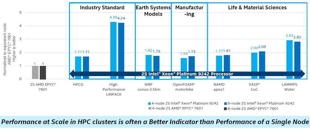
In the benchmarks run above, Intel is using its own S9200WK reference platform, which crams four two-socket Cascade Lake-AP servers into a 2U rack enclosure, which is pretty dense computing by any measure. The servers tested had a pair of the Xeon SP-9242 Platinum processors, which again have 48 cores running at 2.2 GHz, and were are equipped with a measly 256 GB of memory per node using super skinny and supercheap (by comparison anyway) 16 GB DDR4 DIMMs running at 2.93 GHz. The systems have an integrated flash drive for systems software, and link to each other using 48-port Omni-Path 100 switches and adapters, which run at 100 Gb/sec, and they link out to a Lustre parallel file system. They are configured with CentOS 7.7 and the Intel compiler and MPI stacks.
The AMD machines tested were the Supermicro AS-1023US-TR4, which had a pair of the Epyc 7601 processors, which have 32 cores running at 2.2 GHz. They had the same 256 GB of memory configuration (16 x 16 GB), although the memory ran at a slower 2.67 GHz, the top speed that the Epyc 7000 series supports. For whatever reason, Intel put Oracle Linux Server 7.6 on the machines (which is compatible with CentOS 7.6) and in many cases Intel used its own compilers and MPI software on the AMD iron. (We are not sure how much that affected results, but we are skeptical here.) In other cases, the GNU GCC or LLVM/AOCC compilers were used in conjunction with the Intel MPI stack. The AMD systems were linked using 100 GB/sec EDR InfiniBand from Mellanox Technology, and they had a Panasas parallel file system feeding them data.
We agree wholeheartedly with what Intel says at the bottom of the chart, which is that testing clusters of machines is more important than testing single nodes, and would add that you have to test the nodes separately so you have some sense of what peak linear performance would be in a cluster absent latencies in network communication.
This chart shows all kinds of interesting things. First, to our eyes, it doesn’t look like there is much of a difference on these workloads using Omni-Path or InfiniBand. But it is hard to infer that with any precision without seeing the performance of a single node, a two server cluster, and maybe clusters with 16, 32, 64, 128, 256, 512, and 1,024 nodes in addition to the 4 and 8 node clusters tested. We have yet to see any publicly available benchmarks that show the full range of scale so we can make any kind of intelligent assessment of the affect of the onload model of Omni-Path and the offload model of InfiniBand across the full range of standard HPC applications and the typical scales of compute we see at HPC centers in academia, government, and industry.
What this chart also seems to show is how well the Linpack benchmark is taking full advantage of those two FMAs on the AVX-512 units in each core on the Cascade Lake-AP processor, but the tougher HPCG benchmark (which very few machines do well on in terms of computational efficiency, to the point where it is embarrassing for all) does not show as big of a jump in performance over the AMD Epyc 7601 clusters and neither so the WRF weather modeling, OpenFOAM computational fluid dynamics, NAMD molecular dynamics, VASP quantum mechanics, and LAMMP molecular dynamics applications. The latter does better than all of the others, but doesn’t come close to the multiples that Linpack is showing.
If you want to be generous, you could say that the Intel Cascade Lake-AP nodes, with 96 cores per node, are averaging around 2X the performance of the AMD Epyc 7601 nodes, which is the same thing as saying that machines based on the plain vanilla Cascade Lake-SP processors are probably at parity. (The 56-core Cascade Lake-AP chips have about 30 percent more performance on top of that, thanks to more cores and higher clock speeds, but at 400 watts per socket, this is a bridge too far for a lot of HPC shops.) This spread between the Xeon and Epyc processors is consistent with some comparative benchmarks we reviewed out of Intel back in November 2017 pitting Broadwell Xeons and Skylake Xeon SPs against Epyc 7601s.
The question now facing the HPC sector is this: If AMD can deliver 4X the floating point performance, at either 32-bit single precision or 64-bit double precision, with the second generation Rome Epyc processors, how will that theoretical performance, which puts it at parity with the Cascade Lake AP at a socket level and damned near at the core level, translate into performance on the suite of HPC applications that Intel has tested here and on real world HPC applications? With all of the tuning that HPC software makers must have been doing in the past two years, we could see the first real competition in the HPC arena where CPU-only architectures dominate (which is to say most HPC centers outside of the national labs and a few academic centers that try to stay on the cutting edge with accelerators added to their CPUs). It is now going to come down to software tuning by HPC software makers, whether they are commercial codes, open source codes, or homegrown codes. AMD has apparently laid the hardware foundation to compete with Intel, head to head and toe to toe. Now it depends on the software people to take advantage of it.
The big factor in all of this is what Intel does with the future “Ice Lake” Xeon SP processors, to be etched using 10 nanometer processes and to start shipping later this year for a ramp early next year. The “Sunny Cove” cores used in the Ice Lake Xeon SP processors will have pipelines that are both wider to find more parallelism in code and deeper to be able to exploit it. The 10 nanometer shrink will allow more cores to be crammed onto a die, too, and Intel could go even wider with the AVX vector engines (imagine 1,024 bits wide!) or do a full and real implementation of AVX-512 like that in the Xeon Phi chips and not one with the bolt-on FMA that was used in the Skylake, Cascade Lake, and Cooper Lake Xeon SPs.
Don’t count Intel out just yet as we see the AMD market shares rise. We have some real – and it looks like sustainable – competition happening here. And it is exciting.

Being Persistent With Persistent Memory
Intel in October clarified its memory plans moving forward when it announced it is selling its NAND memory business to SK Hynix in a two-step acquisition that is worth $9 billion and will take until 2025 to be completed. However, while the deal itself is unusual – the deal is …

Intel Reorg Puts Gelsinger Firmly In Control Of The Datacenter
Whenever something is not working, you change it. Sometimes, you glue things together to create some sort of synergy and then you pull them apart to get some sort of necessary focus. The pendulum swings back, and forth, and back and forth, creating and destroying value (think building conglomerates and …

Gelsinger Sees Intel’s Foundry As The Future Of Chip Making
This week marked this first time since 2012 that Pat Gelsinger has spoken at the annual Hot Chips conference. Gelsinger is the longtime Intel chief technology officer and former general manager of its Data Center Group, who learned the trade from Intel’s founders and who has returned to be its …
Just like AMD did with its higher clocked 16 core Epyc/Naples 7371, just released in Nov 2018, AMD should probably release a higher clocked 32 core variant and get a bit more performance for the price while awaiting Epyc/Rome’s release and volume ramp starting around middle of this year.
I’m sure that there are plenty of higher binned 14nm/Zen(First Generation) parts that AMD as moved of to the side that can attain some higher clocks in a similar manner to that 16 core 7371 that’s mostly just a better binned part that was saved for just such a targeted market segment that benifts from higher clock speeds.
So AMD can still increase the clocks on some Newer Epyc/Naples SKUs and still not reach 400 Watts TDP. I’m quite certain that GF’s 14nm(Licensed from Samsung) process node has matured enough for AMD to have its binning engineers setting aside the tops for just such an eventuality as is exemplified by the Nov 2018 release of the Epyc/Naples 16 core higher performance variant(7371 SKU).
Zen1 and Epyc/Naples has only 128 bit Floating point units so for any server usage that’s not requiring heavy FP workloads the Power Saved by having smaller AVX like units can go into higher clocks attainable at less total TDP and more affordable cooling options that do not require liquid solutions. Now Zen2 and 256 Bit FP units with the doubling of data paths also and Epyc/Rome at 64 cores will be more for targeting Intel’s top end and Epyc/Naples for some more affordable market segments that will eat away at Intel’s lower server market segments even further.
If I where AMD I would even consider vetting/certifying Epyc/Naples on GF’s 12nm node and bringing to market some even higher clocked Zen+/12nm Epyc/Naples+ SKUs that will still do even better for server workloads where AVX/Heavy FP units are not needed. This is because Epyc/Naples can be made to fill in many of the lower tier value market segments against Intel’s similar offerings. So AMD could Drop the ASPs on any first generation Zen Epyc/Naples lower clocked parts and also introduce some higher clocked Epyc/Naples variants and even a possible 12nm/Zen+ based line of even higher clocked Epyc/Naples+ variants to fill out the middle market segment while Epyc/Rome at 7nm takes the high end duties for any highest margin highest performance segments against Intel’s latest.
TDP and cooling solutions costs also figure in to the TCO metrics and TSMC’s 7nm wafer starts capacity is going to begin to come under pressure as Epyc/Rome and the Phone market more fully moves onto TSMC/7nm production. GF’s 14nm(Samsung) and 12nm production will not have such Wafer Start supply issues and there is still value to be derived from Epyc/Naples for some years to come, in the form of better binned Zen/Zeppelin DIEs that can be turned into higher clocked parts for more affordable server market segments that do not really need or make use of any AVX/FP intensive workloads, and a good many server workloads do not need heavy FP to be productive.
Thanks for this post, a lot of inconsistencies in the AMD side, expected due these are Intel’s benchmarks, the same with the 9900k and with its mythical 28 cores 5ghz demo,also I would like to see if those machines (AMD and Intel) had theirs mitigation agains spectre, I hope that the companies do not fall into that marketing as cheap as the basic user does, we will have to wait for them to reach the market to really test them.
Don’t expect to see a Cassadelake AP solution coming from any major OEMs. The package is a 6,000 pin BGA which Intel will only sell already mounted to their own motherboards.
Likely you will only find re-sellers offering it in whitebox configurations.
Yea,
“For those customers who bought first generation “Skylake” Xeon SP processors, also announced nearly two years ago, there really is not a lot of reason to move on up to Cascade Lake processors of any kind”
XSL those memory starved beasts.
;-}
mb