
Imagine for a second that you are Intel.
The few server CPU makers that remain in the market – AMD, IBM, Marvell, and Ampere – have more memory controllers on their sockets than you do. They are all working towards 7 nanometer chips that are going to cram a lot of cores on the die. Your 10 nanometer process for etching chips, which is analogous to the 7 nanometer technology being offered by Taiwan Semiconductor Manufacturing Corp and being used by three of those vendors (not IBM, which has tapped Samsung), is behind schedule and has spilled some coffee on your roadmap on the way through Lake country. But, the Data Center Group business is booming, even if hyperscalers and cloud builders did tap the brakes in the fourth quarter of 2018. And it is still a long way until the first half of 2020 when the “Ice Lake” Xeons SPs are going to be ramping.
What do you do?
You make the best of it. You tweak the Skylake architecture in a number of ways, and in quick succession, to keep customers moving. This is precisely what Intel did with its Cascade Lake chips today, which we covered in detail here. Intel used a refined 14 nanometer process to squeeze a little more clock speed out of the Skylake cores, added some new DL Boost instructions to speed up machine learning inference, fixed some security hold from the Spectre/Meltdown/Foreshadow speculative execution vulnerabilities, and jiggled the SKU stack so there were a few more cores in a Cascade Lake Xeon SP at a given price point for the original Skylake Xeon SP chips launched nearly two years ago.
But there is only one problem with this strategy. Intel doesn’t get to talk about performance leadership by doing just what is outlined above. Intel needs something more. Just like AMD did with the Opteron 6100s a decade ago when Intel was coming on strong with the “Nehalem” Xeons that are the ancestor of the current Cascade Lakes. AMD put two six-core chips on a die and had a chipset that scaled to eight sockets, and created a physical quad socket server out of eight processors logically linked through its HyperTransport NUMA interconnect.
AMD doubled up the chips in a socket to make a performance statement back then, and Intel is doing it now. With the Cascade Lake-AP processor, Intel is cross coupling four Cascade Lake chips using UltraPath Interconnect, its own NUMA glue, and packaging them in such a way that this logical four socket machine looks like a physical two socket server with monstrous chips. By cramming up to 56 cores onto a single ball grid array (BGA) surface mounted package, Intel can still talk about performance leadership and perhaps even decent price/performance in a two-socket machine ahead of AMD’s “Rome” Epyc server processor launch, which is expected in June if the scuttlebutt is right.
With the Xeon SP 9200 Platinum series of processors, as the Cascade Lake-AP chips are formally known, Intel gets a little experience doing multichip module design and manufacturing, which is good and which is a preview, perhaps, of the way things will ultimately get done in the not too distant future. Making massive monolithic processors is way more costly than making lots more smaller ones, and just like the world had to get used to programming for distributed systems made out of multiple servers, compilers and programmers are going to have to get used to working with distributed systems inside of a single server.
There is no question in anyone’s mind that the future CPU will not only be a hodge-podge of chips, but chips etched with the most optimal processes available for each function. It is highly likely that I/O and communication circuits never get pushed down below 16 nanometers (14 nanometers in the Intel way of counting transistor gate sizes), and that the CPU cores just keep shrinking as much as possible, and that these components will be made of separate chips stitched back together with various kinds of interconnects and packaging methodologies. It would not surprise us at all if Ice Lake Xeon SP chips do this for realsies, and not just in what appears to be the hurried fashion that Intel took with the Cascade Lake-AP chips. Perhaps Intel did not believe that TSMC could get its 7 nanometer act together and therefore AMD did not have a chance with the Rome Epyc processors? It is hard to say.
But at the moment, there is no indication that TSMC is not going to be able to make chips for the many vendors that have lined up to use its 7 nanometer fabs, and AMD looks like it will have a bit of a lead with Rome over Ice Lake – certainly in terms of time to market, and maybe in terms of core count and throughout. We shall have to see.
So think of the Cascade Lake-AP as a glimpse of the future, or at least one where compute density matters and being able to affordably make multichip modules matters even more.
The Slots And Watts
There are four Xeon SP 9200 series chips, which we compared to the rest of the Cascade Lake lineup over here. We already told you about a two chip module based on 24 core Cascade Lake chips last November, and we were expecting for the chip to burn anywhere between 275 watts and 350 watts, depending on what Intel did to the clock speeds on the processors. As it turns out, the clock speeds are a bit higher than many expected on this 48 core part, which is now called the Xeon SP-9242 Platinum, at 2.3 GHz base and a Turbo Boost speed of 3.8 GHz. The lower bin Cascade Lake-AP chips, the Xeon SP-9221 and the Xeon SP-9222, both burn 250 watts and have base clock speeds of 2.1 GHz and 2.3 GHz, respectively, with a turbo up to 3.7 GHz. There are four more cores and therefore eight more threads in these 32 core Cascade Lake-AP parts, and that might be important for certain workloads, but a Xeon SP-8180 in the Skylake family or a Xeon SP-8280 in the plain vanilla Cascade Lake family will give you 28 cores and 56 threads, which is close enough. And we think that the price difference per core is a bit higher on the AP variants than on the regular SKUs with slightly fewer cores. (Again, nothing is free when it comes to chips, unless a competitor is trying to grease the skids of business and reduce friction, as AMD is certainly doing with its Epyc chips.)
The top bin Xeon SP-9282 has two 28 core Cascade Lake chips cohabitating inside of a BGA package. It runs at a base 2.6 GHz and turbos up to 3.8 GHz when it can, and it consumes 400 watts. We think this is the chip everyone was talking about when we heard rumors about a Cascade Lake-AP variant costing more than $20,000 a pop. Intel is not supplying list prices for the Xeon SP-9200 models because they are only available in a complete system designed by Intel, including homegrown motherboards. This is such a different kind of machine that it warrants such special treatment, Kartik Ananth, the Intel senior principal engineer in charge of the S9200WK server node and Server Chassis FC2000 enclosure that uses it, tells The Next Platform. (Nvidia takes the same approach with the NVSwitch interconnect and system boards in its DGX-2 hybrid CPU-GPU components, which are only available from Nvidia itself.)
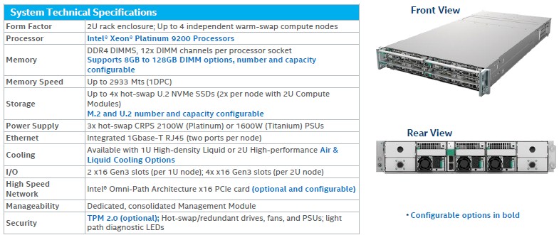
Having a thermal envelope of 250 watts is not that big of a deal – accelerators have been in that range for a decade, but 350 watts is stretching it a bit and it is no surprise to learn that the 400 watt Cascade Lake-AP is only available as a liquid-cooled processor. Putting two of these on a single compute sled, and four of them in a 2U enclosure, it pretty dense in terms of compute and thermals. That’s 3,200 watts and 448 cores in the same size as a normal 2U enclosure that often has an order of magnitude fewer cores in it out there in the enterprise datacenter. If you could get full power to a rack of these, it might take between 64 kilowatts and 122 kilowatts to do the trick, but you would have 8,960 cores per rack; it might cost on the order of $2 million with modest memory configurations and more like $3 million for a beefy setup. (That is an educated, but admittedly wild, guess.)
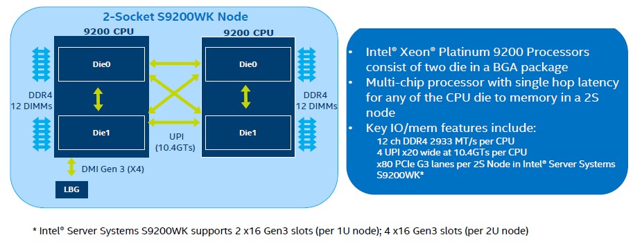
Here is a block diagram showing how the Xeon SP-9200s are logically linked into a two-socket server:
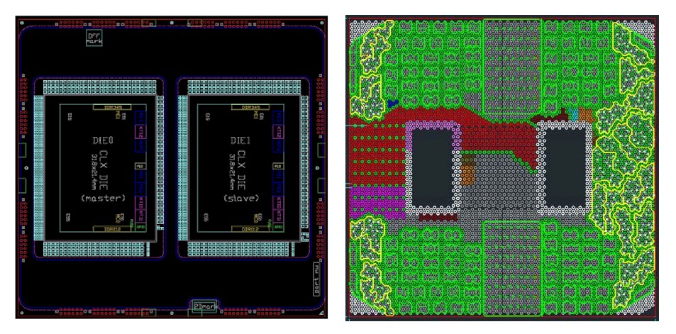
The ball grid array for the Cascade Lake-AP has a whopping 5,903 balls on it, and there is a giant heat spreader that can take the heat off the device. There are six memory channels on each Cascade Lake chip in the BGA, for a total of 12 memory channels per socket, so Intel is in some fashion winning the memory channel and memory bandwidth battle at the “socket” level at this point. But two things to consider. First, you can only have one DDR4 DIMM per channel to run the fast 2.93 GHz memory that the Cascade Lake architecture supports, and doubling up those chips and controllers in the socket does not change the memory bandwidth per core equation one tiny bit. If anything, we need more bandwidth per core, and this does not accomplish this. Other CPU architectures have to make a similar bargain as they add cores but don’t want to add power pins to drive more memory controllers, which consume a lot of power and generate a lot of heat.
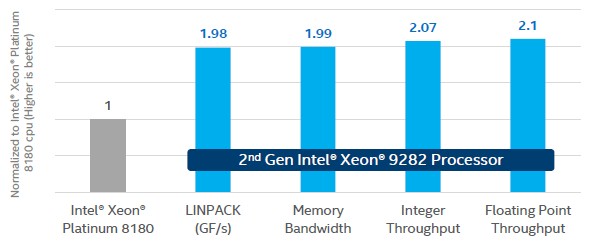
Each Cascade Lake-AP chiplet – can we call such a beast a chiplet? – has three UPI links just like the other Cascade Lake parts, and they run at the top speed 10.4 GT/sec. The links are cross coupled so that one lane is used to link each chip to the other in each BGA package and the remaining four are used to create the NUMA link between the two logical sockets. The topology above is no different than what you would have using UPI links in a quad socket server. Ananth says that it takes about 70 nanoseconds to access memory attached to one processor inside the BGA from the other, but it is about 130 nanoseconds to jump across to the other BGA package in NUMA fashion. It is not clear what kind of performance impact this might have, but generally speaking, the numbers seem about what you expect, with twice as many processors driving twice as much bandwidth. Here is how a Skylake Xeon SP-8180 stacks up against a Cascade Lake-AP Xeon SP-9282:
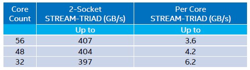
Here is drilled down into memory bandwidth tests, since this is a key aspect of the Cascade Lake-AP sales pitch: The chart below shows the interplay of bandwidth on the STREAM memory test with the number of cores in a two-socket Cascade Lake-AP system:
The Xeon SP-9200 Platinum processors do not, by the way, support Optane 3D XPoint persistent memory modules, which are being touted as a memory extender in the regular “Purley” server platform using regular Cascade Lake processors. In fact, these processors only support a maximum of 768 GB per socket, not even the larger DDR4 memory capacity that some of the other Platinum and Gold series processors in the Skylake and Cascade Lake families do. We saw presentations earlier this year that suggested that some customers might want to use eight of the twelve channels in a socket for DDR4 memory and the remaining four for Optane PMMs, but apparently this must be a custom SKU. There is no technical reason why the Cascade Lake-AP processors can’t support Optane PMMs, as far as we know.
It is interesting to us that this is not being pitched as a search engine SKU, considering that those running search engines generally like to get as many cores in a single system image as possible. (There is a special search engine SKU, as we pointed out in our coverage of the generic Cascade Lake chips, but we think it costs one-tenth as much as that top bin doubled up chip and has only one-third the cores.
Intel’s Cascade Lake-AP Server
It is not clear yet who will be selling servers based on the Xeon SP 9200 processors, but this machine is Intel’s design and OEMs and ODMs pretty much have to take it as it is, and without having space to support for their homegrown, enterprise-grade BMCs. We may see some OEMs do custom engagements, but we don’t expect much action here. This may be where ODMs do the selling, and particularly in China where four-socket machines are popular among the hyperscalers and cloud builders. This is, however, no more compact than a 2U server with four sockets, which has been available for many years. It will all come down to pricing and who will give Intel bragging rights between now and Ice Lake.
In any event, here are the tech specs of the S9200WK enclosure:
And here are the specs for the sleds that go into the enclosure:
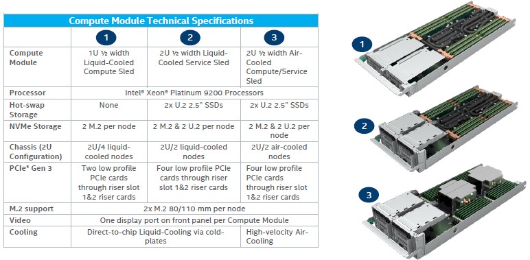 The compute density depends on how much peripheral interconnect and local storage you want on the nodes and whether you have the 400 watt parts or not. Presumably, if you want liquid cooling on the 250 watt or 350 watt parts, just to be efficient, you can do that.
Here is the thing, though. If software is priced by the socket, and if a commercial software vendor will treat the Cascade Lake-AP machine as a two-socket server when, logically it really is a four-socket server, then great. This will definitely drop the VMware and Red Hat bills, and it should be by half on things with socket-based pricing. But if software is priced by the core, the move to the AP processors doesn’t do any good at all, and on homegrown code it makes no difference whatsoever.


With Cloud HPC Toolkit, Google Pursues HPC, Intel Pushes OneAPI
The people running Google Cloud can see the tides of HPC changing and know that, as we discussed only a few months ago, there is a fairly good chance that more HPC workloads will move to cloud builders over time as their sheer scale increasingly dictates future chip and system …
Intel’s Chips No Longer Pay More Than Their Fair Share Of Foundry Costs
The biggest benefit that is coming from the separation of the Intel chip design and marketing business from its foundry operations is that Intel’s chip product groups no longer have to shoulder the totality of the immense costs of its manufacturing operations. The biggest downside is that they these chip …

Who Will Build Europe’s First Exascale Supercomputer – And With What, And Why?
Exascale supercomputing is just as important to Europe as it is to the United States and China, but each of these geopolitical regions on Earth has its own way of developing architectures, funding their development and production, and figuring out where the best HPC centers are to host such machines …
Hello! Nice article, very helpful! Just one question – how do you get to 3,200 Watts per 2U enclosure using the Xeon SP-9282? From my understanding the TDP for the premium-tier Cascade Lake AP is 400W for the full two-chip socket (given that it’s basically two scalable chips glued together with interconnect, and a single premium-tier Cascade Lake SP is 205W).. Which would mean that a dual-socket 2U enclosure would have a power envelope of 800W. Where am I going wrong? All the best.
Or sorry, rather 1,600W if you’re putting four sockets in a 2U enclosure as you suggested. I guess my question is why do you assume a multichip module is 800W, not 400W?