

Updated: AMD’s “Rome” processors, the second generation of Epyc processors that the company will be putting into the field, are a key step for the company on its path back to the datacenter. But AMD is not going to get back into the glass house in a big way with the CPU alone. It is going to take GPUs, too.
The “Vega 20” GPU unveiled this week at AMD’s Next Horizon event in San Francisco will be put into the forthcoming Radeon Instinct MI50 and MI60 accelerators, and is arguably the first GPU in many years that AMD has put into the field that can go head-to-head and toe-to-toe with Nvidia’s GPUs as compute engines. This gives AMD two compute stories to tell, with both CPUs and GPUs, and it also makes AMD the only chip vendor that can put both kinds of compute on the table.
Now comes the task of getting server OEMs and ODMs as well as the major hyperscalers and cloud builders to embrace both kinds of AMD compute. Rome is clearly going to be a lot better than the first generation “Naples” Epyc CPUs, as we have reported elsewhere. And it will certainly be easier to make the case for the forthcoming Vega 20 GPU coming in the Radeon Instinct MI50 and MI60 accelerators than it was for the Vega 10 GPU that came out last year in the MI25 accelerator.
The Vega 10 was good in that it had support for 16-bit floating point math but which had only a modest amount of double precision floating point (1/6th the rate of 32-bit single precision), thus locking it out of a large swath of HPC applications. But the Vega 10 chip, Evan Groenke, senior product manager of the Radeon Instinct line at AMD, was really aimed at visualization and other single precision compute workloads, with some 16-bit machine learning training. The implication is that this is so by design, with AMD gradually building up its credibility in the datacenter and its software stack for HPC and AI workloads for the next generation Vega chips.
Not only does the Vega 20 support 64-bit floating point at half the rate of 32-bit (as it preferred), but the flexible math in the Vega 20 allows for it to support 8-bit, 4-bit, and even 1-bit integer math often used for machine learning inference. The Vega 20 is a much more complete compute engine, and with 32 GB of HBM2 memory and 1 TB/sec of bandwidth into and out of that memory, it can compete well against Nvidia’s top-end “Volta” Tesla V100 accelerators.
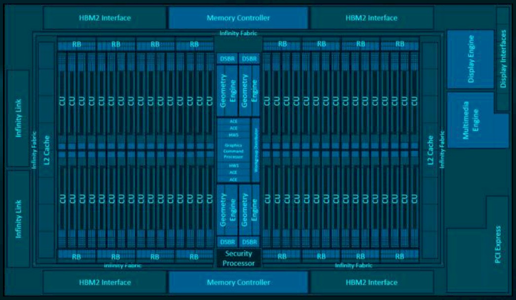
Here is the conceptual block diagram of the Vega 20 chip:

This is a more literal block diagram:
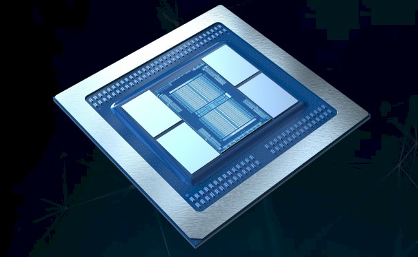
Here is what the Vega 20 GPU looks like with its four banks of HBM2 memory, stacked eight dies high in the top-end part:
And this shows the relative size of the Vega 10 GPU used in the MI25 cards and the Vega 20 GPU used in the MI50 and MI60 cards:
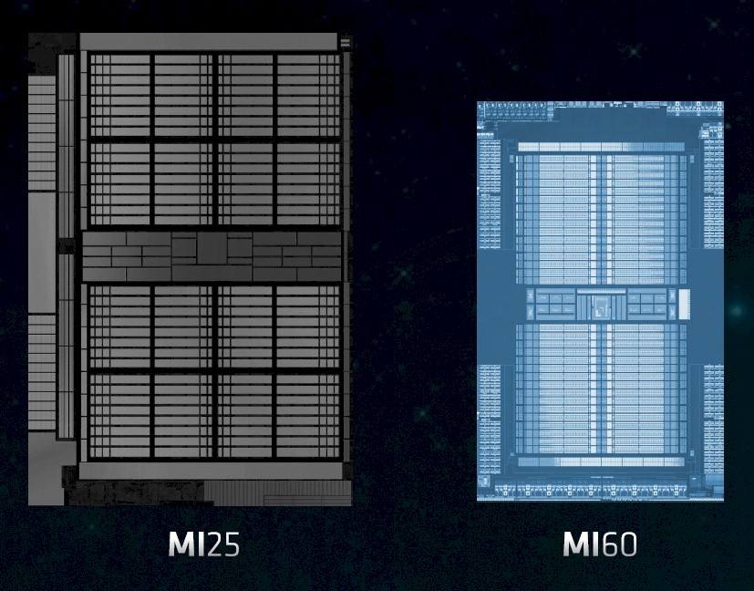
The Vega 20 GPU has 64 compute units on its die, and sports 13.2 billion transistors in a 331 mm2 chip; it is etched using the 7 nanometer manufacturing processes from Taiwan Semiconductor Manufacturing Corp. That is considerably more dense than the Vega 10 chip, which had 12.5 billion transistors in a 500 mm2 chip implemented in 14 nanometer processes, although neither packs the 21.1 billion transistor punch that the Nvidia GV100 GPU used in the Tesla V100 accelerators has; then again, this chip, which is made using 12 nanometer processes from TSMC, advanced two years ago when Volta debuted, weighs in at 815 mm2 area, which is pushing the reticle limit on chip manufacturing.
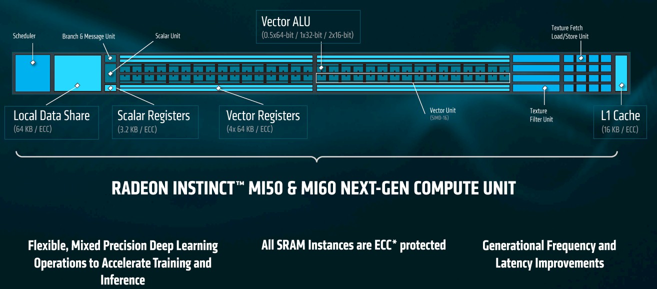
The compute unit at the heart of the Vega 20 design has a mix of scalar (3.2 KB) and vector registers (four banks of 64 KB each to scale from 16-bits up to 64-bits) and a flexible vector math unit plus a local data share that weighs in at 64 KB and an L1 cache for the whole shebang that comes in at 16 KB. It would have been good to have seen such a compute unit design in an AMD GPU many years ago. It is better now than never, and it is clear from the pricing that Nvidia can charge for its Tesla compute engines that the time is overripe for competition.
The full-on Vega 20 chip has 4,096 stream processors across those 64 compute units; it is deployed in the high-end Radeon Instinct MI60 card, which also sports 32 GB of HBM2 memory. There is a variant of the Vega 20 that has only 60 compute units active, which yields 3,840 active stream processors and therefore about 10 percent less performance – presumably at a much lower price point. The MI50 card will also only sport 16 GB of memory, which is what the MI25 card using the Vega 10 chip offered.
The Vega 10 GPU used in the MI25 card clocked at 1.5 GHz, and it looks like the 7 nanometer shrink allowed AMD to push the clocks on the Vega 20 GPUs used in the MI50 and MI60 cards to 1.8 GHz.
Here is how the two Vega 20 cards stack up:

The Vega 20 GPU accelerators will slide into PCI-Express 4.0 slots, and also have Infinity Fabric ports that match those on the Rome Epyc CPUs that are based on the same PCI-Express 4.0 signaling. While the Rome CPUs offer a total of 128 PCI-Express 4.0 lanes, with a total of 512 GB/sec of aggregate bi-directional bandwidth, the Vega 20 cards only eat a single PCI-Express 4.0 x16 slot for 64 GB/sec of that bandwidth, which means you can easily hang four or six of them off a Rome chip, and technically you could do eight if you didn’t need any more peripheral I/O. (Which you do for networking.)
The Vega 20 GPU cards also have an additional pair of PCI-Express 4.0-derived Infinity Fabric ports that come off the accelerators that offer 100 GB/sec of bandwidth each to link the GPU accelerators and their HBM2 memories to each other in a ring structure. This is akin to, but slightly different from, the NVLink interconnect that Nvidia has created to hook GPUs to each other and GPUs to CPUs.
Thanks to those Infinity Fabric ports, AMD is able to show near linear scalability on machine learning training workloads, in this case using the ResNet-50 neural network for image recognition with a batch size of 64. That’s on the right side of this chart:

What everyone will want to know, of course, is how the AMD Vega 20 GPU will stack up against the Nvidia Volta GV100. On raw floating point performance, the devices are pretty comparable:
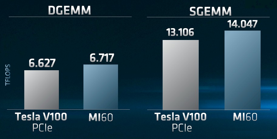
That is definitely within spitting distance on both single precision (SGEMM) and double precision (DGEMM) math benchmarks. Here is how the PCI-Express 3.0 version of the Tesla V100 card stacks up to the Radeon Instinct MI60 on all three benchmarks, which is ResNet-50, SGEMM, and DGEMM:
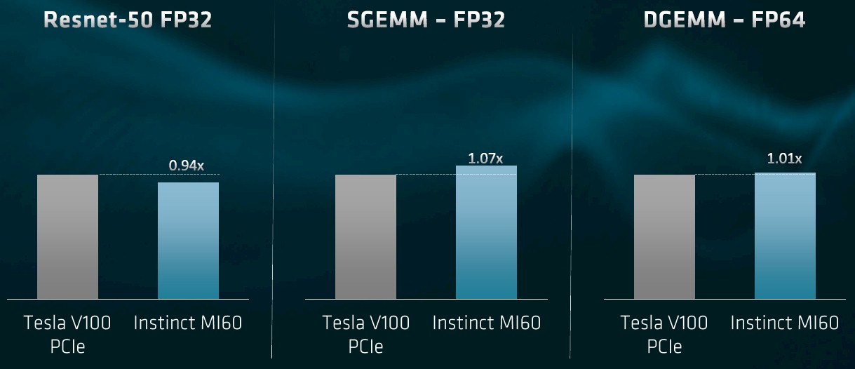
The Tesla V100 is 6 percent ahead of the Radeon Instinct MI60 on machine learning training for image recognition, but the MI60 pulls ahead by 7 percent and 1 percent, respectively, on SGEMM and DGEMM. That’s a pretty tight race, and now the question is what can AMD charge for the Vega 20 cards? We won’t know for quite a while. The MI60 card will be available at the end of the fourth quarter of this year when it ships to the hyperscalers and cloud builders and then gradually becomes available to the rest of the world; the MI50 comes later to the Super Seven in late Q1 2019, to be followed by broader availability.
Update: Nvidia has contested the performance results that AMD presented above, and with absolute justification.
We drilled down into the feeds and speeds of the tests that AMD performed on both the Radeon Instinct MI60 GPU accelerator and the Tesla V100. AMD correctly wanted to compare a PCI-Express card to a PCI-Express card, which is reasonable since it does not have NVLink ports on its Radeon Instinct cards. We all know that using NVLink can significantly improve performance, but neither AMD Epyc nor Intel Xeon processors have NVLink connections between CPUs and GPUs – only the Power9 chip has native NVLink ports.
AMD’s Tesla versus Radeon Instinct plugged a single card of each type into a server with a pair of “Skylake” Xeon SP-6130 Gold processors, and the machines both had 256 GB of memory and were running Ubuntu Server 16.04.5 LTS. The Tesla setup was configured with CUDA 10.0.130 and cuDNN 7.3, which the Radeon Instinct setup was configured with ROCm 19.224. The ResNet-50 image recognition test was run on the TensorFlow 1.11 framework, and use single precision FP32 math units to do the image recognition with a batch size of 256.
Given how close the single precision performance is between the two devices, it is no wonder that AMD saw the performance it did. The only problem – and it is a big one – is that this test completely ignored the Tensor Core matrix multiply and accumulate units, which run in half-precision FP16 and output single-precision FP32. These Tensor Core units absolutely scream on machine learning training workloads. Nvidia revealed just how much back in early May, and these are not results that we saw because that week, to be honest, our daughter was born that week and we were busy. So we did not have that data in our head to be skeptical about. But what is clear, having reviewed that data, is that with the Tensor Cores kicked in, the Tesla V100 whips the AMD Radeon Instinct on ResNet-50 quite handily.
Like this:
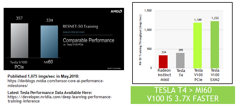
These Nvidia results were obtained running highly optimized neural networks atop the MXNet framework, and the Tesla V100 in a PCI-Express form factor had 4X the performance of the Tesla P100 based on the “Pascal” GPU. The leap in hardware and software together is key here. If you move to an SXM2 implementation of the Tesla V100, the higher bandwidth into and out of the GPU helps goose the performance a little higher, even without direct NVLink ports to the processor. Basically, the AMD Radeon Instinct has about 8 percent more ResNet-50 training performance as the Pascal Tesla V100, and as you can see, even though the new “Turing” T4 accelerator is not really aimed at machine learning training, it can beat the Radeon Instinct MI60 on it because it, too, has those Tensor Cores. By about 19 percent in terms of images per second processed.
None of this takes anything away from the Radeon Instinct when it comes to raw floating point performance at single precision or double precision. So keep that in mind. And unless and until HPC-style codes start using Tensor Cores instead of floating point units, these AMD GPUs are absolutely competitive with the Tesla GPUs for such work. But clearly AMD needs to have a matrix multiply and accumulate unit to be competitive with Nvidia on machine learning training.
We eagerly await doing the price/performance comparisons across these enterprise GPU compute engines.


AMD Deepens Its Already Broad Epyc Server Chip Roadmap
The hyperscalers, cloud builders, HPC centers, and OEM server manufacturers of the world who build servers for everyone else all want, more than anything else, competition between component suppliers and a regular, predictable, almost boring cadence of new component introductions. This way, everyone can consume on a regular schedule and …
Chip Roadmaps Unfold, Crisscrossing And Interconnecting, At AMD
After its acquisitions of ATI in 2006 and the maturation of its discrete GPUs with the Instinct line from the past few years and the acquisitions of Xilinx and Pensando here in 2022, AMD is not just a second source of X86 processors. Now, without question, it is a formidable …
The Steady Patience Of AMD In The Datacenter
We have said more than once in recent weeks that recessions accelerate technology transitions but they do not cause them. We now have a textbook experimental case developing between AMD and Intel where it concerns CPUs for servers and where it concerns GPUs and both AMD’s and Intel’s desires to …
@Author,
Using 7nm to match nVidia, does AMD have architecture problems?
It’s a much smaller chip than the GV100. However, they are probably also dependent on the thermal advantage of 7 nm to compete with the GV100, so there probably is an architectural issue there. But it doesn’t match NVIDIA because it doesn’t have anything to match Tensor Cores.
This chip isn’t really practical competition, it is only the first step in an attempt to enter the competition, assuming AMD continues to make the investment into hardware and software in the space. The MI60 probably won’t have good availability for months, and then it’s going to have to be validated. By the time it could show up for widespread usage NVIDIA’s next generation architecture on 7 nm will be knocking on the door. Then there is also the big gap in software optimization and support to consider.
Volta is so big it’s dangerous… It is at the optical limit for 12nm (815mm) so even a full shrink would still have it at around 500mm (12nm is not twice 7nm…
“12nm is not twice 7nm…”
Traditionally, you would have been wrong, as a 10nm part should have 2x the density of 14nm(10/14 squared equals ~0.5).
But with all foundries turning such numbers into marketing, it doesn’t mean much anymore.
According to the information above, 14nm doesn’t offer 2x density over 7nm either.
14nm = 12.5 billion transistors, 500mm2
7nm = 13.2 billion transistors, 331mm2
Traditionally, 7nm should have 4x the density of 14nm.
No. You should compare by die area and the number of transistors used. 13 billion vs 21 billion, and 331 mm2 vs 815 mm2. Do the math. Not to mention price.
We must consider how many transistors the 3 NVLink controllers use.
But when the AMD chip has so much less utility do to an inferior toolchain, inferior application optimization, and lack of Tensor Cores the greater cost to manufacture of NVIDIA’s chip is not that big of a deal.
The ResNet-50 numbers from AMD are bogus, they avoided FP16 precision and thus Volta didn’t get to use it’s power Tensor Cores. That would have made it much faster than Vega 20.
Also AMD used the PCI-E V100, this is the slowest V100 available, There is V100 NVlink, which is at least 10% faster than PCI-E V100.
Then again, some of us (HPC physics) are concerned only with fp64 + bandwidth, so AMD have our attention. Price-wars? Good times?