

This year at the International Supercomputing Conference (ISC) Dr. Keren Bergman from the Lightwave Research Lab at Columbia University detailed the road ahead for optical interconnects in supercomputing and what it means for exascale energy efficiency and beyond.
The power consumption of Summit, the top performing supercomputer according to this summer’s most recent Top 500 rankings, is 13MW for 122 petaflops of peak performance. Summit like other machines tends toward heavier, fatter nodes with a lot of in-node horsepower and relatively thin interconnect bandwidth outside since it is focused on local computation.
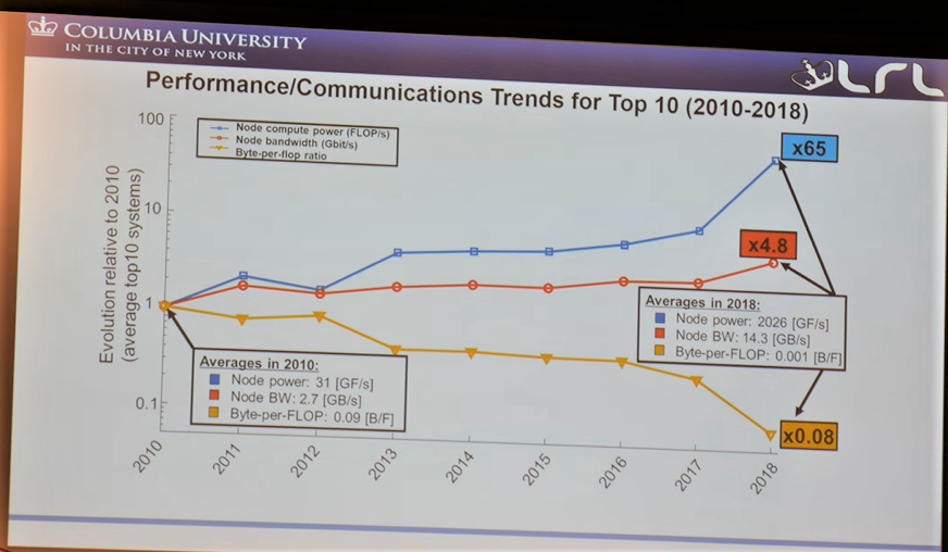
Bergman points out that since 2010, the node compute power (based on Top 500 systems) has grown by 65X. In that same span, bandwidth has only grown 5X and when it comes to a byte per flop ratio, there has been an actual decrease of almost 1X.
With that in mind, data movement penalties for accessing DRAM and SRAM are not heavy but when it comes to moving to more common memory elements like HBM for instance, it gets more expensive against the exascale power budget. In short, scaling performance under tight energy restrictions means improvement in data movement are still needed. Bergman argues that a novel interconnect is at the heart of exascale efficiency, especially with more accelerated architectures in on large supercomputers and for that matter, systems built for AI training.
So, what can photonics bring to the table for HPC?
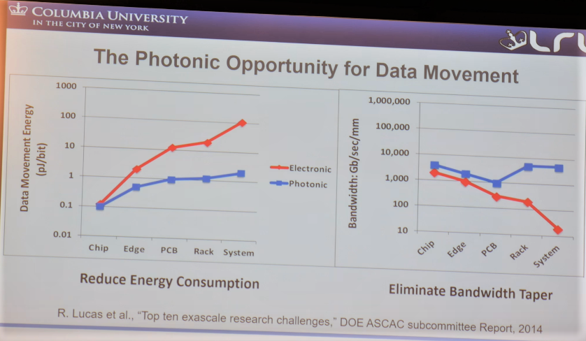
To begin with, optical interconnects are driven by electronics—driving the bits from the laser, detecting them, etc. all takes electronic circuitry. That means the baseline energy cost is always the same as electronic interconnects but the real difference is that optics don’t require reamplification or regeneration. The energy consumption can remain more or less flat and so what is being spent at the chip level is in theory the same it would be at the system level.
But how can HPC implement this and once it is in place, what is the best way to maximize the data movement benefits?
Photons are obviously different than electronics so some things require a rethink while being what Bergman calls “minimally invasive” to application owners. The goal is to make photonics look electronic from a software standpoint while reworking areas where optics are different (for instance, they don’t switch the same way, no optical buffers or packet switching, etc.).
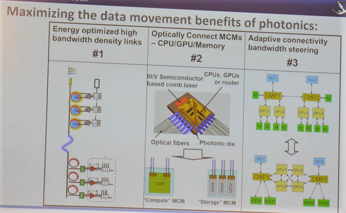
Bergman says reaching this point has three stages—the first is to squeeze the most density and energy efficiency out as possible and then, with those bandwidth dense links are place, connect those to compute elements (memory, CPU, GPU) so the systems can be disaggregated for even further energy savings. In essence, the final state is being able to dial the topology however the application wants it-whether that’s a string of GPUs only or a fully interconnected system.
Bergman and her team at Columbia through partnerships with HPE and a number of other vendors are working on an interconnect that is prime for HPC deployments. In essence, this optical fabric will be scalable to a terabits per second per millimeter of bandwidth density with work to minimize link losses and penalties, refine channel picking, and optimizing fabrication with AIM as a partner. Eventually with the optical fabric connecting the various components on systems, it is possible to send things only when needed to enable an architecture that is a network of resources, not a stacked on. In other words, it is more efficient and flexible.
Optical interconnects can fit many wavelengths in the same propagation waveguide or fiber because photons can bunch together and go any distance. The laser source (this one interestingly can be powered by a single AAA battery) creates the wavelengths and gets imprinted with data from a ring resonator module. The optical link with its encoded data is then propagated with relatively low loss.
Begman compares this approach to NVLink in the chart below.
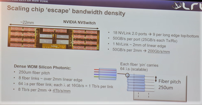
NVLink is the most dense of the interconnects with NVSwitch having 18 links versus the optical “pins” on the other device with their many wavelengths. Optical interconnects can have 1 Tb/s per pin in optical I/O which leads to TB/s mm metrics listed here with room for scalability.
The real benefit beyond this is simply that resources can be disaggregated for GPU-cnetric workloads, for example, which is where the promise lies. However, even though applications should not have to be changed dramatically if at all to make up for the new communication patterns, retooling code to allow this efficiently will be important for some workloads.
More on Bergman’s work can be found here.

Photonics To Make Celestial HBM3 Memory Fabric
There is no shortage of silicon photonics technologies under development, and every few months it seems like another startup crops up promising massive bandwidth, over longer distances, while using less power than copper interconnects. Celestial AI is the latest contender to enter this space, having popped back up after a …

Celestial AI Wants To Break The Memory Wall, Fuse HBM With DDR5
In 2024, there is no shortage of interconnects if you need to stitch tens, hundreds, thousands, or even tens of thousands of accelerators together. Nvidia has NVLink and InfiniBand. Google’s TPU pods talk to one another using optical circuit switches (OCS). AMD has its Infinity Fabric for die-to-die, chip-to-chip, and …

A Five-Year Challenge Roadmap for Photonics-Based Computing
Silicon photonics has been proving its worth in telco and communications but there is a much brighter opportunity photonics-based computing. The energy efficiency and data movement potential is promising, especially for increasingly data-laden analytics and AI/ML applications, but the road to a diverse hardware ecosystem for compute is still long. …
Be the first to comment