

We have profiled a number of processor updates and novel architectures this week in the wake of the Hot Chips conference this week, many of which have focused on clever FPGA implementations, specialized ASICs, or additions to well-known architectures, including Power and ARM.
Among the presentations that provided yet another way to loop around the Moore’s Law wall is a 1,000-core processor “KiloCore” from UC Davis researchers, which they noted during Hot Chips (and the press repeated) was the first to wrap 1000 processors on a single die. Actually, Japanese startup, Exascaler, Inc. beat them to this with the PEZY-SC (a 28nm MIMD processor with 1,024 cores and has rankings on the Green 500 and a few machine wins in the country). This hiccup aside, the MIMD-based KiloCore approach is interesting–and has some noteworthy results compared to similar efforts.
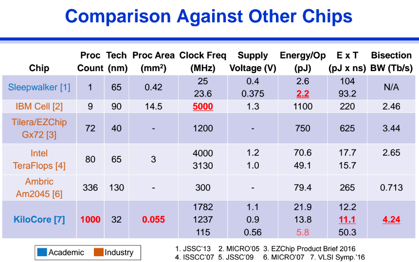
KiloCore has proven successful on both energy consumption and performance fronts. As one of the leads, Dr. Bevan Baas, shared from Hot Chips, the processors-per-die curve has remained relatively static over the last several years—with KiloCore representing a huge leap in the chart below.

The trajectory above is nothing new for Dr. Bevan Baas, who has spent decades immersed in low-power, high performance processor design before becoming a professor at UC Davis. In the late 80s he was one of the designers of a high-end minicomputer in HP’s Computer Systems Division, before joining Atheros Communications, where he helped develop the first IEEE 802.11a wifi LAN. He now focuses on algorithms, architectures and circuits as part of the VLSI Computation Lab at UC Davis.
“KiloCore has been designed with the needs of computationally-intensive applications and kernels in mind. It is meant to act as a co-processor within a larger system and isn’t intended to run an operating system itself. There could be some cases in applications or systems where it could act as a sole processor, but they wouldn’t be general purpose systems,” Baas explains.
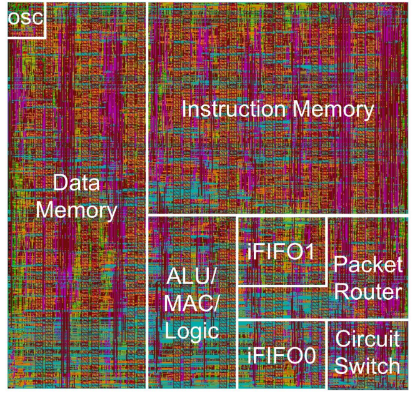
Each processor holds up to 128 instructions (and those larger are supported for the processors next to a shared memory block). Those are modified during application programming and stacked during runtime. The idea is to program them at once, stack them together, and let them go, Baas says. Applications can also optionally request that processors be reprogrammed during runtime based on signals from the processors—so a processor might get to a point in execution and send a package to the administrator with a reprogramming request. Alternately, groups of processors can do the same. “Most applications we have tested don’t’ use or need this feature, but it is possible,” Baas notes.
Data is passed via messages between processors (which means they don’t need to hop through a processor’s memory). The messages move from processor A’s software to the other’s software. At its simplest, it is a read/write with synchronization step between the processors, which is part of what makes it possible to scale to thousands, or even tens of thousands of processors, with the programmer needing to worry about synchronization routines and the like—the goal is that “they sort themselves out,” according to Baas.
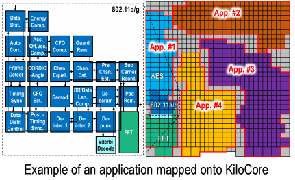 One final word about programming. The way applications are implemented fits the architecture well. They are broken down into min-programs that are 128 words or less via a set of steps where the small programs are isolated down to coarse-grained tasks, task code is partitioned into serial code blocks, and parallelizable code blocks are replicated. Ultimately, this means a KiloCore array can run several different tasks at once, as seen in the example pictured. This sounds easy enough in a brief explanation, but one has to imagine there’s some significant development overhead.
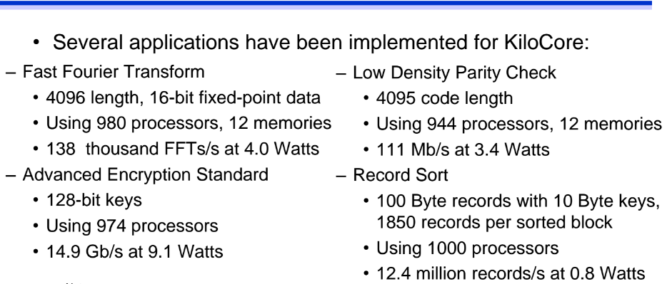
In essence, this is more of an instruction coprocessor versus one capable of doing heavy-handed math, but there are places where this can be useful. For instance, as Bevan describes, they have particular lucj with some key applications as pictured below.
So where does the idea of a “killer core” really come into play? It could be in the future. This is a 32nm chip and that means, if they continue using IBM’s processor, they have steps from 32 to 22 and then 14, with each step allowing the addition of far more transistors and a kick to the clock potential. That could be 2.5X jump with 2500 cores in a 40 watt thermal envelope with the ability to manage 4.5 billion instructions per second using steps from Global Foundries. That is, of course, assuming it can scale.
As it stands now, KiloCore has a nice trajectory–although sadly, one would be hard-pressed to find several of these on the market.
The full paper describing results and architecture, as well as far more about the memory structure (which is worth a look) can be found here.


PEZY currently has spots #1 and #2 on the Green500, and has for a while now, and is actually going well beyond 1024 cores soon.
In 2017 they’re due to release a 4096 PEZY cores and 12 MIPS64 cores, 8.1 DP TFLOPS chip with 32GB of “UltraMemory” and 256GB of DDR4, sort of like Knights Landing in memory arrangement.
The UltraMemory is using the wireless, induction based ThruChip Interface, which itself is a very interesting alternative to TSVs for communication between dies, and highly doped TSVs to deliver power to the DRAM.
The most impressive thing is that with 4x64Gbit stacks the bandwidth is 4.1TB/s. Apparently, that chip will be made using the relatively mature TSMC 16nm FinFET process that’s already being extensively used by Nvidia.
Interesting I wonder how well PEZY would do on Deep Learning algorithms mostly SGD the heavy part of the algorithm but even using FFT for convolution. The power envelop seems very impressive. Question is how does the memory bandwidth stack up.